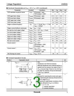
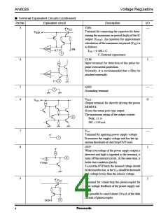
Voltage Regulators
AN8026
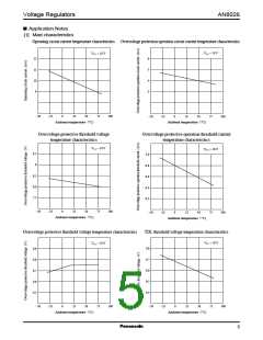
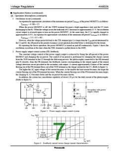
■ Application Notes (continued)
[2] Operation descriptions (continued)
2. Oscillation circuit (continued)
An equation for approximate calculation of the maximum on-period TON(max) of the power MOSFET is as follows:
ON(max) = 6 500 × C3
T
When the power MOSFET is off, the TOFF terminal becomes a high impedance state and the C2 starts
discharging by the R2. When the voltage across the both ends of C2 decreases to approximately 0.1 V, the oscillation
circuit output is reversed again to turn on the power MOSFET. At the same time, the C2 is rapidly charged to
approximately 0.9 V. An equation for approximate calculation of the minimum off-period TOFF(min) is as follows:
T
OFF(min) = 2.2 × C2 × R2
However, when the voltage-period fed back to the TDL terminal (pin 1) is longer than the TOFF period determined by
the C2 and R2, the off-period in the pseudo-resonance circuit operation described below is determined by the former.
By repeating the above operation, the power MOSFET is turned on and off continuously. Figure 2 shows the
oscillation waveform at the time when the TDL terminal is pulled down to the GND.
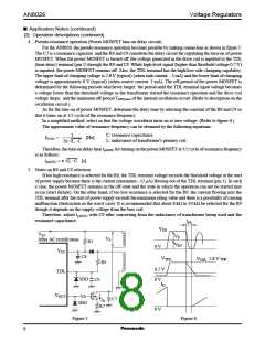
3. Power supply output control system (FB: feedback)
The constant voltage control of the power supply output is achieved by fixing the off-period of the power
MOSFET and changing the on-period. The control of on-period is performed by changing the charge current
from the TON terminal to the C3 through the following process: the photocoupler connected to the FB terminal
(pin 9) absorbs, from the FB terminal, the feedback current corresponding to the output signal of the output
voltage detection circuit provided in the secondary side output. A current approximately 8 times of the current
flowing out of the FB terminal flows out of the TON terminal as the charge current for the C3. (Refer to figure 3.)
The higher the AC input voltage of the current becomes, or the smaller the load current becomes, the larger the
current flowing out of the FB terminal becomes. When the current flowing out of the FB terminal becomes larger,
the charging to C3 becomes faster and the on-period becomes shorter.
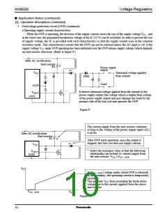
In addition, the system has cancellation capability of about 150 µA for the dark current of the photocoupler.
(Refer to figure 4.)
1:8
Secondary side power
supply output
PC
200 Ω
AN1431T/M
PC
C3 C2
R2
Primary
side
Secondary
side
Figure 3. Power supply output control system
ITON (mA)
−10
−8
−6
−4
−2
Dark
current
0
− 0.2
− 0.4
− 0.6
− 0.8
−1.0
IFB (mA)
Figure 4. Feedback current versus charge current characteristics
7

 PANASONIC [ PANASONIC ]