Voltage Regulators
AN8026
■ Application Notes (continued)
[2] Operation descriptions (continued)
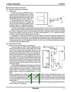
8. Output block
In order to drive the power MOSFET which is
a capacitive load at high speed, this IC is adopt-
ing the totem pole (push-pull) type output circuit
which performs the sink and source of the current
with the NPN transistor as shown in figure 10.
The maximum sink/source current is ±0.1 A
(DC) and the current at peak is ±1.0 A (peak). The
circuit is provided with the sink capability even if
the supply voltage VCC is under the stop voltage so
that it turns off the power MOSFET without fail.
Schottky barrier
diode
Figure 10
The peak current capability is mainly required and a particularly too large current is not required constantly.
Because the power MOSFET which becomes a load for the output is capacitive, a large peak current is required
for driving it at a high speed. However, after the charge and discharge, a particularly large current is not required
to keep such condition. In the case of this IC, the peak current capability of ±1 A is ensured by taking a
capacitance value of the power MOSFET used into account.
The parasitic LC of the power MOSFET may produce ringing to decrease the output pin under the GND
potential. When the voltage decrease of the output pin becomes larger than the voltage drop of diode and its
voltage becomes negative, the parasitic diode consisting of the substrate and collector of the output NPN turns on.
This phenomenon can cause the malfunction of device. In such a case, the Schottky barrier diode should be
connected between the output and GND.
[3] Design reference data
• How to start the soft start function by external parts
The power supply rises under overload condition due to the
capacitor connected to the power supply output. In this condi-
tion, since the voltage of the power supply output is low, the
normal constant voltage control attempts to rise the power sup-
ply output at the maximum duty. The control uses the pulse-by-
pulse overcurrent protection (CLM), attempting to limit the cur-
rent. However, the pulse can not be brought down to zero due to
delay of filter, etc. As a result, a large current flows into the main
switch (the power MOSFET) or the diode in the secondary side,
and in the worst case these parts are damaged. For this reason,
the soft start function is used to suppress the rush current at start
of the power supply.
As the method of installing the soft start function, the R3 and
C4 are connected between the OVP terminal (pin 8) and the
CLM terminal (pin 4) as shown in figure 11. When the supply
voltage of the IC reaches the start voltage and the start circuit
begins to operate, an open bias of approximately 6.5 V at the
OVP
After AC rectification
Start resistor
R1
VCC
C8
OVP
C4
R3
VOUT
CLM
R6
GND
C6
R7
Figure 11
terminal is outputted. By this voltage, the charge current flows into the C4 and the CLM terminal voltage rises. The
CLM terminal voltage decreases with the lapse of time since it changes in proportion to the charge current of the
C4. The CLM circuit operates by the sum of the voltage across the both ends of R7 created by the current flowing
into the power MOSFET when turning on power and the voltage across the both ends of R6 created by the charge
current of the C4.
Therefore, since the current which flows into the power MOSFET when turning on power gradually increases,
the rush current can be suppressed.
11

 PANASONIC [ PANASONIC ]