PFS122
8bit MTP MCU with 12-bit R-Type ADC
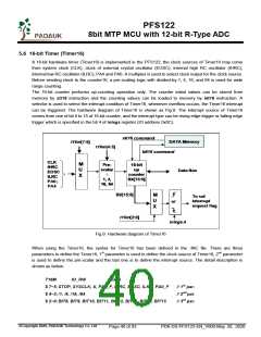
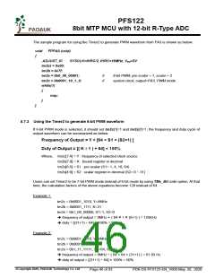
5.7 8-bit Timer (Timer2/Timer3) with PWM generation
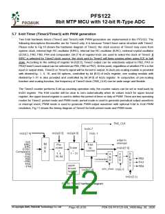
Two 8-bit hardware timers (Timer2 and Timer3) with PWM generation are implemented in the PFS122. The
following descriptions thereinafter are for Timer2 only. It is because Timer3 have same structure with Timer2.
Please refer to Fig.10 shown the hardware diagram of Timer2, the clock sources of Timer2 may come from
system clock, internal high RC oscillator (IHRC), internal low RC oscillator (ILRC), external crystal oscillator
(EOSC), PA0, PB0, PA4 and comparator. Bit [7:4] of register tm2c are used to select the clock of Timer2. If
IHRC is selected for Timer2 clock source, the clock sent to Timer2 will keep running when using ICE in halt
state. According to the setting of register tm2c[3:2], Timer2 output can be selectively output to PB2, PA3 or
PB4(Timer3 count output can be selected as PB5, PB6 or PB7). At this point, regardless of whether PX.x is the
input or output state, Timer2( or Timer3) signal will be forced to output. A clock pre-scaling module is provided
with divided-by- 1, 4, 16, and 64 options, controlled by bit [6:5] of tm2s register; one scaling module with
divided-by-1~31 is also provided and controlled by bit [4:0] of tm2s register. In conjunction of pre-scaling
function and scaling function, the frequency of Timer2 clock (TM2_CLK) can be wide range and flexible.
The Timer2 counter performs 8-bit up-counting operation only; the counter values can be set or read back by
tm2ct register. The 8-bit counter will be clear to zero automatically when its values reach for upper bound
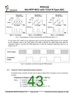
register, the upper bound register is used to define the period of timer or duty of PWM. There are two operating
modes for Timer2: period mode and PWM mode; period mode is used to generate periodical output waveform
or interrupt event; PWM mode is used to generate PWM output waveform with optional 6-bit to 8-bit PWM
resolution, Fig.11 shows the timing diagram of Timer2 for both period mode and PWM mode.
Fig.10: Timer2 hardware diagram
©Copyright 2020, PADAUK Technology Co. Ltd
Page 42 of 93
PDK-DS-PFS122-EN_V000-May 28, 2020

 PADAUK [ PADAUK Technology ]