OXCB950
OXFORD SEMICONDUCTOR LTD.
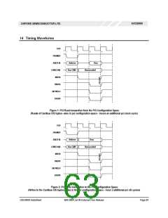
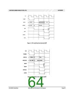
14 Timing Waveforms
CLK
FRAME#
AD[31:0]
C/BE[3:0]#
IRDY#
1
2
3
4
Address
Data
Bus CMD
Byte enable#
TRDY#
DEVSEL#
STOP#
Figure 1: PCI Read transaction from the PCI Configuration Space
(Reads of Cardbus CIS tuples –also in pci configuration space- incurs an additional pci clock cycle)
CLK
1
2
3
4
FRAME#
AD[31:0]
C/BE[3:0]#
IRDY#
Address
Data
Bus CMD
Byte enable#
TRDY#
DEVSEL#
STOP#
Figure 2: PCI Write transaction to the PCI Configuration Space
(Writes to the Cardbus CIS tuples – also in the pci configuration space - incur 2 additional pci clk cycles)
OXCB950 DataSheet
MIS-0004 Jul 04 External-Free Release
Page 63

 OXFORD [ OXFORD SEMICONDUCTOR ]