OXCB950
OXFORD SEMICONDUCTOR LTD.
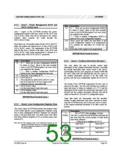
CKS[6]: Transmitter clock source selector
7.11.7 Device Identification Registers
logic 0 ⇒ The transmitter clock source is the output of the
baud rate generator (550 compatibility).
logic 1 ⇒ The transmitter uses an external clock applied
to the RI# pin.
The identification registers is located at offsets 0x08 to
0x0B of the ICR
The UARTs offer four bytes of device identification. The
device ID registers may be read using offset values 0x08 to
0x0B of the Indexed Control Register. Registers ID1, ID2
and ID3 identify the device as an OX16C950 and return
0x16, 0xC9 and 0x50 respectively. The REV register
resides at offset 0x0B of ICR and identifies the revision of
950 core. This register returns 0x05 for revision A of the
OX1CB950.
CKS[7]: Transmitter 1x clock mode selector
logic 0 ⇒ The transmitter is in Nx clock mode as defined
in the TCR register. After a hardware reset the
transmitter operates in 16x clock mode, i.e.
16C550 compatibility.
logic 1 ⇒ The transmitter is in isochronous 1x clock
mode.
7.11.8 Clock Select Register ‘CKS’
7.11.9 Nine-bit Mode Register ‘NMR’
The CKS register is located at offset 0x03 of the ICR
The NMR register is located at offset 0x0D of the ICR
This register is cleared to 0x00 after a hardware reset to
maintain compatibility with 16C550, but is unaffected by
software reset. This allows the user to select a clock
source and then reset the channel to work-around any
timing glitches.
The UART offers 9-bit data framing for industrial multi-drop
applications. The 9-bit mode is enabled by setting bit 0 of
the Nine-bit Mode Register (NMR). In 9-bit mode the data
length setting in LCR[1:0] is ignored. Furthermore as parity
is permanently disabled, the setting of LCR[5:3] is also
ignored.
CKS[1:0]: Receiver Clock Source Selector
logic [00] ⇒ The RCLK pin is selected for the receiver
clock (550 compatible mode).
The receiver stores the 9th bit of the received data in
LSR[2] (where parity error is stored in normal mode). Note
that the UART provides a 128-deep FIFO for LSR[3:0].
The transmitter FIFO is 9 bits wide and 128 deep. The user
should write the 9th (MSB) data bit in SPR[0] first and then
write the other 8 bits to THR.
logic [01] ⇒ The DSR# pin is selected for the receiver
clock.
logic [10] ⇒ The output of baud rate generator (internal
BDOUT#) is selected for the receiver clock.
logic [11] ⇒ The transmitter clock is selected for the
receiver. This allows RI# to be used for both
transmitter and receiver.
As parity mode is disabled, LSR[7] is set whenever there is
an overrun, framing error or received break condition. It is
unaffected by the contents of LSR[2] (Now the received 9th
data bit).
CKS[2]: Reserved
In 9-bit mode, in-band flow control is disabled regardless of
the setting of EFR[3:0] and the XON1/XON2/XOFF1 and
XOFF2 registers are used for special character detection.
CKS[3]: Receiver 1x clock mode selector
logic 0 ⇒ The receiver is in Nx clock mode as defined in
the TCR register. After a hardware reset the
receiver operates in 16x clock mode, i.e.
16C550 compatibility.
Interrupts in 9-Bit Mode:
While IER[2] is set, upon receiving a character with status
error, a level 1 interrupt is asserted when the character and
the associated status are transferred to the FIFO.
logic 1 ⇒ The receiver is in isochronous 1x clock mode.
CKS[5:4]: Transmitter 1x clock or baud rate generator
output (BDOUT) on DTR# pin
The UART can assert an optional interrupt if a received
logic [00] ⇒ The function of the DTR# pin is defined by
the setting of ACR[4:3].
th
character has its 9 bit set. As multi-drop systems often
th
use the 9 bit as an address bit, the receiver is able to
logic [01] ⇒ The transmitter 1x clock (bit rate clock) is
asserted on the DTR# pin and the setting of
ACR[4:3] is ignored.
generate an interrupt upon receiving an address character.
This feature is enabled by setting NMR[2]. This will result
in a level 1 interrupt being asserted when the address
character is transferred to the receiver FIFO.
logic [10] ⇒ The output of baud rate generator (Nx clock)
is asserted on the DTR# pin and the setting
of ACR[4:3] is ignored.
In this case, as long as there are no errors pending, i.e.
LSR[1], LSR[3], and LSR[4] are clear, '0' can be read back
from LSR[7] and LSR[1], thus differentiating between an
‘address’ interrupt and receiver error or overrun interrupt in
logic [11] ⇒ Reserved.
DS-0033 Sep 05
External-Free Release
Page 49

 OXFORD [ OXFORD SEMICONDUCTOR ]