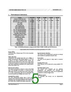
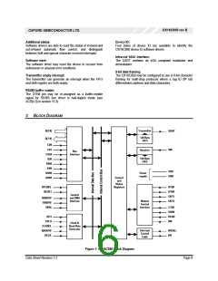
OX16C950 rev B
OXFORD SEMICONDUCTOR LTD.
PLCC TQFP Dir1 Name
Serial port pins
Description
13
8
O
SOUT
Transmitter serial data output.
IrDA_Out
This pin is re-defined to IrDA output when IrDA mode is enabled, i.e. MCR[6]
set in Enhanced mode.
O
O
36
32
RTS#
DTR#
Active-low Request-To-Send output. Whenever the automated RTS# flow
control is enabled, the RTS# pin is de-asserted and re-asserted if the receiver
FIFO reaches or falls below a pair of programmed flow control thresholds,
respectively. This pin’s state is controlled by bit 1 of the MCR. RTS may also
be used as a general-purpose output.
Active-low modem Data-Terminal-Ready output. Whenever the automated
DTR# flow control is enabled, the DTR# pin is asserted and de-asserted if the
receiver FIFO reaches or falls below a pair of programmed flow control
thresholds, respectively. The state is set by bit 0 of the MCR. DTR may also
be used as a general purpose output.
37
33
O
O
485_EN
In RS485 half-duplex mode, the DTR# pin may be programmed to reflect the
state of the transmitter empty bit (or it’s inverse) to automatically control the
direction of the RS485 transceiver buffer (see ACR[4:3]).
Tx_Clk_Out
Transmitter 1x (or baud rate generator output) clock. For isochronous
applications, the 1x (or Nx) transmitter clock may be asserted on the DTR#
pin (see CKS[5:4]).
O
I
11
40
7
SIN
Receiver serial data input.
I
IrDA_In
This pin is re-defined to IrDA input when IrDA mode is enabled, i.e. MCR[6]
set in Enhanced mode.
38
I
CTS#
Active-low Clear-To-Send input. Whenever the automated CTS# flow control
is enabled and the CTS# pin is de-asserted, the transmitter will complete the
current character and enter the idle mode until the CTS# pin is re-asserted.
However, flow control characters are transmitted regardless of the state of the
CTS# pin. The state of this pin is reflected in bit 4 of the MSR. It can also be
used as a general-purpose input.
41
39
I
DSR#
Active-low modem Data-Set-Ready input. Whenever the automated DSR#
flow control is enabled and the DSR# pin is de-asserted, the transmitter will
complete the current character and enter the idle mode until the DSR# pin is
re-asserted. However, flow control characters are transmitted regardless of
the state of the DSR# pin. The state of this pin is reflected in bit 5 of the
MSR. It can also be used as a genera- purpose input.
I
I
I
Rx_Clk_In External receiver clock for isochronous applications. The Rx_Clk_In is
selected when CKS[1:0] = ‘01’.
42
43
40
41
DCD#
Active-low modem Data-Carrier-Detect input. The state of this pin is reflected
in bit 7 of the MSR. It can also be used as a general-purpose input
Active-low modem Ring-Indicator input. The state of this pin is reflected in bit
6 of the MSR. It can also be used as a general-purpose input. RI can be
configured as tx and rx for a 1x clock in isochronous operation.
RI#
I
Tx_Clk_In External transmitter clock. This clock can be used by the transmitter (and by
the receiver indirectly) when CKS[6]=’1’.
17
12
5
O
BDOUT#
Baud out. BDOUT# is a Nx (usually 16x, see TCR) clock signal for the
transmitter. It is the output of the baud generator module. The receiver can
use this clock by connecting BDOUT# to the RCLK pin or setting CKS[1:0] to
’10’ where BDOUT# will be connected to RCLK internally. In this case setting
CKS[2] to ‘1’ will disable the BDOUT# pin to conserve power.
Receiver clock. RCLK is the Nx (usually 16x, see TCR) baud rate clock for
the receiver.
10
I
RCLK
Data Sheet Revision 1.2
Page 9

 OXFORD [ OXFORD SEMICONDUCTOR ]