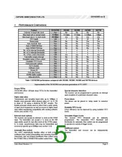
OX16C950 rev B
OXFORD SEMICONDUCTOR LTD.
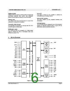
PIN DESCRIPTIONS
4
PLCC
Clock
18
TQFP
14
Dir1 Name
Description
I
XTLI
Crystal oscillator input or external clock pin.
Maximum frequency 60 MHz @ 5V, 50 MHz @ 3.3V
19
23
15
O
IU
XTLO
CLKSEL
Crystal oscillator output. Not used when an alternative TTL level clock is
applied to XTLI and can be left unconnected.
21
The state of this pin on power up configures the internal clock prescaler. This
pin has an internal pull-up. When CLKSEL pin is high the pre-scalar is
bypassed. Connect this pin to GND to enable the internal clock prescaler
(see section 14.2). The complement of this pin is loaded in MCR[7] after a
hardware reset.
This pin can also be used as an alternative external clock pin under software
control (replacing XTLI and thus reducing noise/power due to XTLO) for
embedded applications
Processor Interface
39
35
I
I
RESET
Active-high hardware reset. Hardware reset is described in section 7.1. This
pin must be tied inactive when not in use.
14, 15
16
29 -31 26 – 28
28
9,
10
11
CS0,CS1 Active-high chip select. All chip select pins must be active for the device to
be selected.
CS2#
A[2:0]
ADS#
I
I
I
Active-low chip select.
Address lines to select channel registers.
24
Active-low address strobe. When ADS# signal is low, the address (A[2:0])
and chip select signal (CS0, CS1, CS2#) drive the internal logic, otherwise
they are latched at the level they were when low-to-high transition of ADS#
signal occurred. This pin is used when address and chip selects are not
stable during read or write cycles. If this functionality is not required, this pin
can be permanently tied to GND.
9 - 2
26
4 – 2,
47 – 43
22
I/O
O
I
DB[7:0]
DDIS
Eight-bit 3-state data bus.
Drive Disable. This pin goes active (high) when CPU is not reading from
OX16C950. This signal can be used to disable an external transceiver.
Active-low write strobe. When IOW# is used to write the chip, IOW should be
tied low (inactive).
20
16
IOW#
21
24
17
19
I
I
IOW
Active-high write strobe. When IOW is used to write the chip, IOW# should be
tied high (inactive).
Active-low read strobe. When IOR# is used to read from the chip, IOR should
be tied low (inactive).
IOR#
25
20
I
IOR
Active-high read strobe. When IOR is used to read from the chip, IOR#
should be tied high (inactive).
Data Sheet Revision 1.2
Page 8

 OXFORD [ OXFORD SEMICONDUCTOR ]