OX16C950 rev B
OXFORD SEMICONDUCTOR LTD.
PLCC TQFP
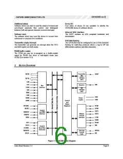
Interrupt & DMA Pins
Dir1 Name
Description
33
30
O
INT
The serial channel has a three-state interrupt output. This signal goes active
(high) when an interrupt condition occurs. The three-state logic is controlled
by INTSEL# and MCR[3] as described below.
27
32
34
23
29
36
O
O
IU
TXRDY#
RXRDY#
INTSEL#
Signal for DMA transfer of transmitter data. There are two modes of DMA
signalling described in section 8.1.
Signal for DMA transfer of received data. There are two modes of DMA
signalling described in section 8.1.
Active-low interrupt select. This pin has an internal pull-up resistor. When
INTSEL# is high or unconnected, the INT pin is enabled and MCR[3] is
ignored. When INTSEL# is low, the tri-state control of INT is controlled by
MCR[3]. In this case INT is enabled when MCR[3] is set and is high-
impedance when MCR[3] is low.
This pin is used to save the external three-state buffer for the interrupt pin.
When using this facility, the INT output should be pulled down to GND using
a 1KΩ resistor.
Miscellaneous Pins
38
35
1
34
31
37
O
O
ID
OUT1#
OUT2#
FIFOSEL
This user defined output pin reflects the complement of MCR[2]. It is inactive
(high) after a hardware reset or during loopback mode.
This user defined output pin reflects the complement of MCR[3]. It is inactive
(high) after a hardware reset or during loopback mode
FIFO select. This pin has an internal pull-down. For backward compatibility
with 16C550, 16C650 and 16C750 devices the FIFO depth is 16 when
FIFOSEL is low or left open. The FIFO size is 128 when FIFOSEL is high.
The unlatched state of this pin is readable by software. The FIFO size may
be set to 128 by writing a 1 in FCR[5] when LCR[7] is set or by putting the
device into Enhanced mode, thus overriding the state of the FIFOSEL pin.
This pin is unconnected in 16C550 and 16C750 devices.
-
48
ID
VSEL
Voltage selector. This pin is used to control the voltage thresholds on all
input pins. When low (or unconnected), 5V biased TTL thresholds are used.
When high, 3V biased TTL thresholds are used. Generally should be tied
high when the OX16C950 is being powered off 3 Volts, and low (or
unconnected) when powered off 5 Volts. If tied high under 5V operation,
CMOS compatible input thresholds are obtained.
As this pin is not accessible in the PLCC, the PLCC is unsuitable for 3V
applications.
12
1, 13,
25, 6
NC
These pins are not connected.
Power and Ground
22
18
GND
VDD
Ground (0 Volts). The GND pin should be tied to ground.
Power supply. The VDD pin should be tied to 5 Volts or 3.3 Volts
Table 2: Pin Descriptions
44
42
Note 1: Direction key:
I
Input
IU
ID
O
Input with pull-up
Input with pull-down
Output
I/O
Bi-directional
Note: Attention should be given to high frequency decoupling of power and ground pins due to the high frequency internal switching that occurs
under normal operation
Data Sheet Revision 1.2
Page 10

 OXFORD [ OXFORD SEMICONDUCTOR ]