UC3844, UC3845, UC2844, UC2845
Undervoltage Lockout
designer added flexibility in tailoring the drive voltage
independent of V A zener clamp is typically connected
to this input when driving power MOSFETs in systems
Two undervoltage lockout comparators have been
incorporated to guarantee that the IC is fully functional
before the output stage is enabled. The positive power
supply terminal (V and the reference output (V ) are
CC.
where V is greater the 20 V. Figure 23 shows proper
CC
power and control ground connections in a current sensing
power MOSFET application.
CC
ref
each monitored by separate comparators. Each has built−in
hysteresis to prevent erratic output behavior as their
respective thresholds are crossed. The V
upper and lower thresholds are 16 V/10 V for the UCX844,
comparator
CC
Reference
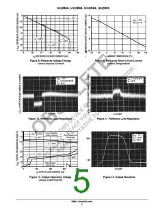
The 5.0 V bandgap reference is trimmed to ± 1.0%
tolerance at T = 25°C on the UC284X, and ± 2.0% on the
and 8.4 V/7.6 V for the UCX845. The V comparator upper
ref
J
and lower thresholds are 3.6 V/3/4 V. The large hysteresis
and low startup current of the UCX844 makes it ideally
suited in off−line converter applications where efficient
bootstrap startup techniques later required (Figure 30). The
UCX845 is intended for lower voltage DC−to−DC converter
applications. A 36 V zener is connected as a shunt regulator
UC384X. Its primary purpose is to supply charging current
to the oscillator timing capacitor. The reference has short
circuit protection and is capable of providing in excess of
20 mA for powering additional control system circuitry.
Design Considerations
from V to ground. Its purpose is to protect the IC from
CC
Do not attempt to construct the converter on
wire−wrap or plug−in prototype boards. High frequency
circuit layout techniques are imperative to prevent
pulsewidth jitter. This is usually caused by excessive noise
pick−up imposed on the Current Sense or Voltage Feedback
inputs. Noise immunity can be improved by lowering circuit
impedances at these points. The printed circuit layout should
contain a ground plane with low−current signal and
high−current switch and output grounds returning on
separate paths back to the input filter capacitor. Ceramic
excessive voltage that can occur during system startup. The
minimum operating voltage for the UCX844 is 11 V and
8.2 V for the UCX845.
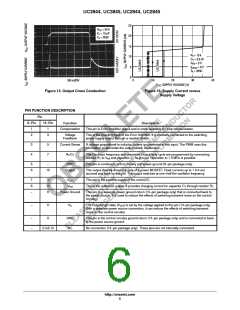
Output
These devices contain a single totem pole output stage that
was specifically designed for direct drive of power
MOSFETs. It is capable of up to ± 1.0 A peak drive current
and has a typical rise and fall time of 50 ns with a 1.0 nF load.
Additional internal circuitry has been added to keep the
Output in a sinking mode whenever and undervoltage
lockout is active. This characteristic eliminates the need for
an external pull−down resistor.
bypass capacitors (0.1 mF) connected directly to V , V ,
CC
C
and V may be required depending upon circuit layout.
ref
This provides a low impedance path for filtering the high
frequency noise. All high current loops should be kept as
short as possible using heavy copper runs to minimize
radiated EMI. The Error Amp compensation circuitry and
the converter output voltage divider should be located close
to the IC and as far as possible from the power switch and
other noise generating components.
The SOIC−14 surface mount package provides separate
pins for V (output supply) and Power Ground. Proper
C
implementation will significantly reduce the level of
switching transient noise imposed on the control circuitry.
This becomes particularly useful when reducing the I
pk(max)
clamp level. The separate V supply input allows the
C
V
ref
8(14)
R
R
8(14)
4(7)
R
R
Bias
R
A
R
T
Bias
4
8
R
B
5.0k
6
OSC
+
−
External
Sync
Input
OSC
+
4(7)
R
S
C
T
3
0.01
+
5
2
Q
+
+
−
−
+
2R
7
EA
47
−
2(3)
1(1)
2R
R
5.0k
1
EA
2(3)
1(1)
C
MC1455
R
5(9)
5(9)
To
Additional
UCX84XA’s
R
B
1.44
(R + 2R )C
The diode clamp is required if the Sync amplitude is large enough to
cause the bottom side of CT to go more than 300 mV below ground.
f =
D
max
=
R
A
+ 2R
B
A
B
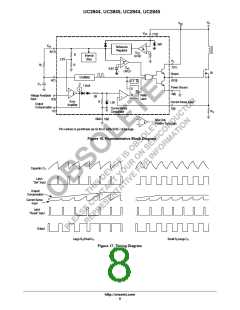
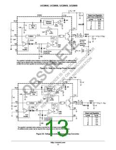
Figure 18. External Clock Synchronization
Figure 19. External Duty Cycle Clamp and
Multi−Unit Synchronization
http://onsemi.com
9

 ONSEMI [ ONSEMI ]