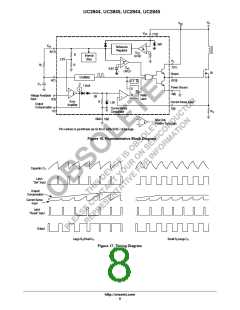
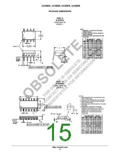
UC3844, UC3845, UC2844, UC2845
V
CC
I
B
V
in
V
in
7(12)
+
0
−
+
5.0V
Base
Charge
Removal
ref
−
+
−
+
C
1
−
+
7(11)
6(10)
5(8)
R
g
−
Q1
Q1
T
6(1)
5(8)
S
Q
−
R
+
Comp/Latch
3(5)
3(5)
R
S
R
S
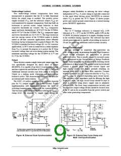
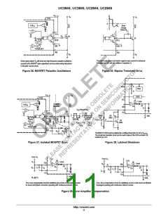
The totem−pole output can furnish negative base current for enhanced
transistor turn−off, with the addition of capacitor C .
1
Series gate resistor R will damp any high frequency parasitic oscillations
g
caused by the MOSFET input capacitance and any series wiring inductance
in the gate−source circuit.
Figure 25. MOSFET Parasitic Oscillations
Figure 26. Bipolar Transistor Drive
8(14)
4(7)
R
R
Bias
V
CC
V
in
OSC
7(12)
+
1.0mA
2R
+
+
Isolation
Boundary
−
5.0V
ref
−
+
EA
2(3)
1(1)
R
−
+
V
Waveforms
GS
−
Q1
+
7(11)
6(10)
5(8)
+
0
−
+
0
−
−
2N
3905
MCR
101
5(9)
T
50% DC
V
25% DC
2N
3903
S
− 1.4
N
N
(pin 1)
P
Q
−
I
=
pk
R
+
S
3 R
S
R
Comp/Latch
3(5)
C
N
S
R
S
N
p
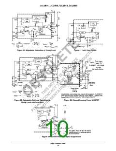
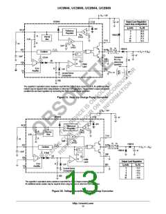
The MCR101 SCR must be selected for a holding of less than 0.5 mA at T
.
A(min)
The simple two transistor circuit can be used in place of the SCR as shown. All
resistors are 10 k.
Figure 27. Isolated MOSFET Drive
Figure 28. Latched Shutdown
From V
O
From V
2.5V
O
+
2.5V
+
R
1.0mA
2R
i
2(3)
1.0mA
2R
+
R
p
2(3)
R
−
i
+
−
EA
R
d
C
I
R
f
EA
R
C
I
R
R
f
d
R
C
p
1(1)
1(1)
5(9)
R ≥ 8.8 k
f
5(9)
Error Amp compensation circuit for stabilizing any current−mode topology except
for boost and flyback converters operating with continuous inductor current.
Error Amp compensation circuit for stabilizing current−mode boost and flyback
topologies operating with continuous inductor current.
Figure 29. Error Amplifier Compensation
http://onsemi.com
11

 ONSEMI [ ONSEMI ]