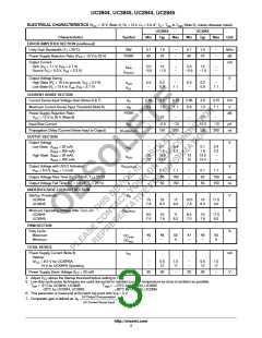
UC3844, UC3845, UC2844, UC2845
OPERATING DESCRIPTION
The UC3844, UC3845 series are high performance, fixed
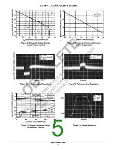
This occurs when the power supply is operating and the load
is removed, or at the beginning of a soft−start interval
(Figures 21, 22). The Error Amp minimum feedback
resistance is limited by the amplifier’s source current
frequency, current mode controllers. They are specifically
designed for Off−Line and DC−to−DC converter
applications offering the designer a cost effective solution
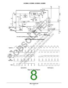
with minimal external components. A representative block
diagram is shown in Figure 16.
(0.5 mA) and the required output voltage (V ) to reach the
OH
comparator’s 1.0 V clamp level:
3.0 (1.0 V) + 1.4 V
Rf(min)
≈
= 8800 W
Oscillator
0.5 mA
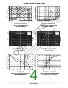
The oscillator frequency is programmed by the values
selected for the timing components R and C . Capacitor C
Current Sense Comparator and PWM Latch
T
T
T
is charged from the 5.0 V reference through resistor R to
approximately 2.8 V and discharged to 1.2 V by an internal
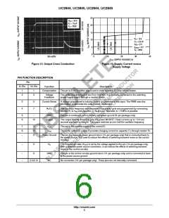
The UC3844, UC3845 operate as a current mode
controller, whereby output switch conduction is initiated by
the oscillator and terminated when the peak inductor current
reaches the threshold level established by the Error
Amplifier Output/Compensation (Pin 1). Thus the error
signal controls the inductor current on a cycle−by−cycle
basis. The current Sense Comparator PWM Latch
configuration used ensures that only a single pulse appears
at the Output during any given oscillator cycle. The inductor
current is converted to a voltage by inserting the ground
T
current sink. During the discharge of C , the oscillator
T
generates an internal blanking pulse that holds the center
input of the NOR gate high. This causes the Output to be in
a low state, thus producing a controlled amount of output
deadtime. An internal flip−flop has been incorporated in the
UCX844/5 which blanks the output off every other clock
cycle by holding one of the inputs of the NOR gate high. This
in combination with the C discharge period yields output
T
deadtimes programmable from 50% to 70%. Figure 2 shows
referenced sense resistor R in series with the source of
S
R
T
versus Oscillator Frequency and Figure 3, Output
output switch Q1. This voltage is monitored by the Current
Sense Input (Pin 3) and compared a level derived from the
Error Amp Output. The peak inductor current under normal
operating conditions is controlled by the voltage at pin 1
where:
Deadtime versus Frequency, both for given values of C .
T
Note that many values of R and C will give the same
T
T
oscillator frequency but only one combination will yield a
specific output deadtime at a given frequency.
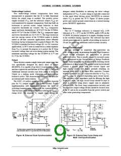
In many noise sensitive applications it may be desirable to
frequency−lock the converter to an external system clock.
This can be accomplished by applying a clock signal to the
circuit shown in Figure 18. For reliable locking, the
free−running oscillator frequency should be set about 10%
less than the clock frequency. A method for multi unit
synchronization is shown in Figure 19. By tailoring the
clock waveform, accurate Output duty cycle clamping can
be achieved to realize output deadtimes of greater than 70%.
V(Pin 1) − 1.4 V
Ipk
=
3 RS
Abnormal operating conditions occur when the power
supply output is overloaded or if output voltage sensing is
lost. Under these conditions, the Current Sense Comparator
threshold will be internally clamped to 1.0 V. Therefore the
maximum peak switch current is:
1.0 V
RS
Ipk(max)
=
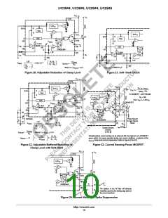
When designing a high power switching regulator it
becomes desirable to reduce the internal clamp voltage in
Error Amplifier
A fully compensated Error Amplifier with access to the
inverting input and output is provided. It features a typical
dc voltage gain of 90 dB, and a unity gain bandwidth of
1.0 MHz with 57 degrees of phase margin (Figure 6). The
noninverting input is internally biased at 2.5 V and is not
pinned out. The converter output voltage is typically divided
down and monitored by the inverting input. The maximum
input bias current is −2.0 mA which can cause an output
voltage error that is equal to the product of the input bias
current and the equivalent input divider source resistance.
The Error Amp Output (Pin 1) is provide for external loop
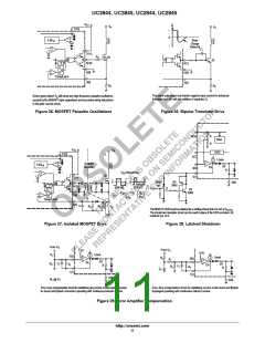
compensation (Figure 29). The output voltage is offset by
two diode drops (≈ 1.4 V) and divided by three before it
connects to the inverting input of the Current Sense
Comparator. This guarantees that no drive pulses appear at
order to keep the power dissipation of R to a reasonable
S
level. A simple method to adjust this voltage is shown in
Figure 20. The two external diodes are used to compensate
the internal diodes yielding a constant clamp voltage over
temperature. Erratic operation due to noise pickup can result
if there is an excessive reduction of the I
voltage.
clamp
pk(max)
A narrow spike on the leading edge of the current
waveform can usually be observed and may cause the power
supply to exhibit an instability when the output is lightly
loaded. This spike is due to the power transformer
interwinding capacitance and output rectifier recovery time.
The addition of an RC filter on the Current Sense Input with
a time constant that approximates the spike duration will
usually eliminate the instability; refer to Figure 24.
the Output (Pin 6) when Pin 1 is at its lowest state (V ).
OL
http://onsemi.com
7

 ONSEMI [ ONSEMI ]