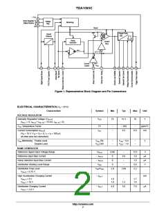
TDA1085C
+ V
CC
9
10
8
Shunt Regulator
Ballast Resistor
Voltage
Reg
Monitoring
Reset
Trigger Pulse
Gen.
Speed
Detector
−
+
Ramp
Generator
Control
Amp
=
0.7 V
Current
Limiter
−V
CC
12
11
4
5
6
3
7
16
14
15
2
1
13
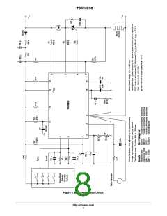
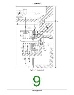
Figure 1. Representative Block Diagram and Pin Connections
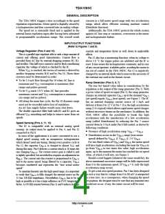
ELECTRICAL CHARACTERISTICS (T = 25°C)
A
Characteristic
Symbol
Min
Typ
Max
Unit
VOLTAGE REGULATOR
Internally Regulated Voltage (V
)
V
15
15.3
16
V
Pin 9
CC
(I
= 0, I
+ I
= 15 mA, I
= 0)
Pin 13
Pin 7
Pin 9
Pin 10
V
Temperature Factor
TF
−
−
− 100
4.5
−
ppm/°C
CC
Current Consumption (I
)
I
6.0
mA
Pin 9
CC
(V = 15 V, V = V = 0, I = I = 100 mA,
9
12
8
1
2
all other pins not connected)
V
V
Monitoring Enable Level
Monitoring Disable Level
V
EN
−
−
V
V
− 0.4
− 1.0
−
−
V
CC
CC
CC
CC
CC
V
DIS
CC
RAMP GENERATOR
Reference Speed Input Voltage Range
Reference Input Bias Current
Ramp Selection Input Bias Current
Distribution Starting Level Range
Distribution Final Level
V
0.08
0
−
13.5
1.0
1.0
2.0
2.2
V
mA
mA
V
Pin 5
− I
− I
0.8
−
Pin 5
Pin 6
0
V
0
−
DS
V
/V
2.0
2.09
DF DS
V
= 0.75 V
Pin 6
High Acceleration Charging Current
− I
mA
Pin 7
Pin 7
V
V
= 0 V
1.0
1.0
−
1.7
1.4
Pin 7
Pin 7
= 10 V
1.2
Distribution Charging Current
= 2.0 V
− I
4.0
5.0
7.0
mA
V
Pin 7
http://onsemi.com
2

 ONSEMI [ ONSEMI ]