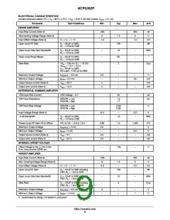
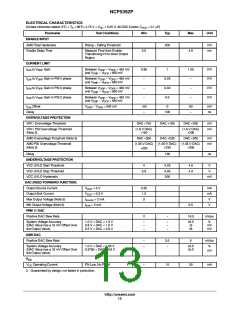
NCP5392P
ELECTRICAL CHARACTERISTICS
(Unless otherwise stated: 0°C < T < 85°C; 4.75 V < V < 5.25 V; All DAC Codes; C
= 0.1 mF)
A
CC
VCC
Parameter
ERROR AMPLIFIER
Input Bias Current (Note 3)
Test Conditions
Min
Typ
Max
Unit
-200
0
200
3
nA
V
Noninverting Voltage Range (Note 3)
Input Offset Voltage (Note 3)
Open Loop DC Gain
1.3
-
V+ = V- = 1.1 V
C = 60 pF to GND,
R = 10 KW to GND
-1.0
-
1.0
mV
dB
100
L
L
Open Loop Unity Gain Bandwidth
Open Loop Phase Margin
Slew Rate
C = 60 pF to GND,
L
R = 10 KW to GND
-
-
-
10
80
5
-
-
-
MHz
°
L
C = 60 pF to GND,
L
R = 10 KW to GND
L
DV = 100 mV, G = - 10 V/V,
in
DV = 1.5 V – 2.5 V,
V/ms
out
C = 60 pF to GND,
L
DC Load = 125 mA to GND
Maximum Output Voltage
Minimum Output Voltage
I
I
= 2.0 mA
3.5
-
-
-
-
-
-
50
-
V
SOURCE
= 0.2 mA
mV
mA
mA
SINK
Output source current (Note 3)
Output sink current (Note 3)
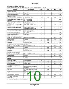
DIFFERENTIAL SUMMING AMPLIFIER
VSN Input Bias Current
V
= 3.5 V
2
out
V
= 1.0 V
2
-
out
VSN Voltage = 0 V
30
mA
kW
VSP Input Resistance
DRVON = Low
DRVON = High
1.5
17
VSP Input Bias Voltage
DRVON = Low
DRVON = High
0.09
0.66
V
Input Voltage Range (Note 3)
-3 dB Bandwidth
-0.3
-
-
3.0
-
V
C = 80 pF to GND,
L
R = 10 KW to GND
10
MHz
L
Closed Loop DC Gain VS to Diffout
Maximum Output Voltage
VS+ to VS- = 0.5 to 1.6 V
0.98
3.0
-
1.0
-
1.025
V/V
V
I
= 2 mA
-
0.5
-
SOURCE
Minimum Output Voltage
I
= 2 mA
-
V
SINK
Output source current (Note 3)
Output sink current (Note 3)
INTERNAL OFFSET VOLTAGE
V
out
= 3 V
2.0
2.0
-
mA
mA
V
out
= 0.5 V
-
-
Offset Voltage to the (+) Pin of the
Error Amp and the VDRP pin
-
1.30
-
V
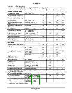
VDROOP AMPLIFIER
Input Bias Current (Note 3)
Non-inverting Voltage Range (Note 3)
Input Offset Voltage (Note 3)
Open Loop DC Gain
-200
0
200
3
nA
V
1.3
-
V+ = V- = 1.1 V
C = 20 pF to GND including
ESD, R = 1 kW to GND
-4.0
-
4.0
mV
dB
100
L
L
Open Loop Unity Gain Bandwidth
Slew Rate
C = 20 pF to GND including
L
ESD, R = 1 kW to GND
-
-
10
5
-
-
MHz
L
C = 20 pF to GND including
L
ESD, R = 1 kW to GND
V/ms
L
Maximum Output Voltage
Minimum Output Voltage
I
I
= 4.0 mA
3
-
-
-
-
1
V
V
SOURCE
= 1.0 mA
SINK
3. Guaranteed by design, not tested in production.
http://onsemi.com
9

 ONSEMI [ ONSEMI ]