NCP5392P
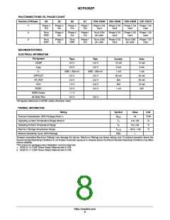
PIN CONNECTIONS VS. PHASE COUNT
Number of Phases
G4
G3
G2
G1
CS4-CS4N
CS3-CS3N
CS2-CS2N
CS1-CS1N
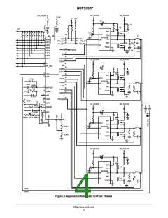
4
Phase 4
Out
Phase 3
Out
Phase 2
Out
Phase 1
Out
Phase 4 CS
input
Phase 3 CS
input
Phase 2 CS
input
Phase 1 CS
input
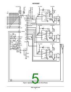
3
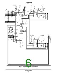
2
Tie to
GND
Phase 3
Out
Phase 2
Out
Phase 1
Out
Tie to CSN
pin used
Phase 3 CS
input
Phase 2 CS
input
Phase 1 CS
input
Tie to
GND
Phase 2
Out
Tie to
GND
Phase 1
Out
Tie to CSN
pin used
Phase 2 CS
input
Tie to CSN
pin used
Phase 1 CS
input
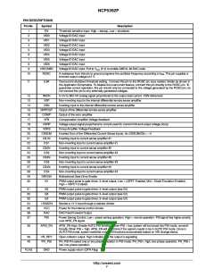
MAXIMUM RATINGS
ELECTRICAL INFORMATION
Pin Symbol
V
MAX
V
MIN
I
I
SINK
SOURCE
COMP
5.5 V
5.5 V
-0.3 V
10 mA
10 mA
V
DRP
-0.3 V
5 mA
1 mA
20 mA
N/A
5 mA
1 mA
20 mA
20 mA
10 mA
N/A
V–
GND + 300 mV
5.5 V
GND – 300 mV
-0.3 V
DIFFOUT
VR_RDY
VCC
5.5 V
-0.3 V
7.0 V
-0.3 V
N/A
ROSC
5.5 V
-0.3 V
1 mA
IMON Output
All Other Pins
1.1 V
5.5 V
-0.3 V
*All signals referenced to AGND unless otherwise noted.
THERMAL INFORMATION
Rating
Symbol
Value
34
Unit
°C/W
°C
Thermal Characteristic, QFN Package (Note 1)
Operating Junction Temperature Range (Note 2)
Operating Ambient Temperature Range
Maximum Storage Temperature Range
Moisture Sensitivity Level, QFN Package
R
q
JA
T
J
0 to 125
0 to +85
-55 to +150
1
T
A
°C
T
STG
°C
MSL
Stresses exceeding Maximum Ratings may damage the device. Maximum Ratings are stress ratings only. Functional operation above the
RecommendedOperating Conditions is not implied. Extended exposure to stresses above the Recommended Operating Conditions may affect
device reliability.
*The maximum package power dissipation must be observed.
1. JESD 51-5 (1S2P Direct-Attach Method) with 0 LFM.
2. JESD 51-7 (1S2P Direct-Attach Method) with 0 LFM.
http://onsemi.com
8

 ONSEMI [ ONSEMI ]