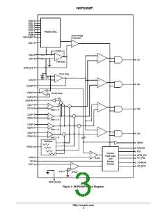
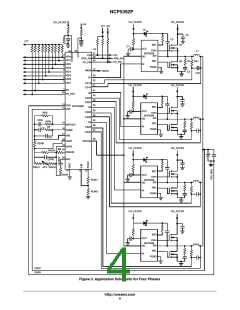
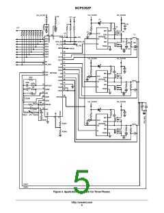
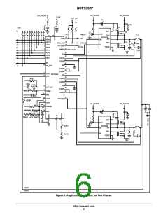
NCP5392P
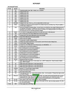
PIN DESCRIPTIONS
Pin No.
Symbol
EN
Description
1
2
Threshold sensitive input. High = startup, Low = shutdown.
Voltage ID DAC input
VID0
3
VID1
Voltage ID DAC input
4
VID2
Voltage ID DAC input
5
VID3
Voltage ID DAC input
6
VID4
Voltage ID DAC input
7
VID5
Voltage ID DAC input
8
VID6
Voltage ID DAC input
9
VID7/AMD
ROSC
Voltage ID DAC input. Pull to V (5 V) to enable AMD 6-bit DAC code.
CC
10
A resistance from this pin to ground programs the oscillator frequency according to f . This pin supplies a
SW
trimmed output voltage of 2 V.
11
ILIM
Overcurrent shutdown threshold setting. Connect this pin to the ROSC pin via a resistor divider as shown in
the Application Schematics. To disable the overcurrent feature, connect this pin directly to the ROSC pin. To
guarantee correct operation, this pin should only be connected to the voltage generated by the ROSC pin; do
not connect this pin to any externally generated voltages.
12
13
14
15
16
17
18
19
20
21
22
23
24
25
26
27
28
29
30
IMON
VSP
0 mV to 900 mV analog signal proportional to the output load current. VSN referenced
Non-inverting input to the internal differential remote sense amplifier
Inverting input to the internal differential remote sense amplifier
Output of the differential remote sense amplifier
Output of the error amplifier
VSN
DIFFOUT
COMP
VFB
Compensation Amplifier Voltage feedback
VDRP
VDFB
CSSUM
CS1N
CS1
Voltage output signal proportional to current used for current limit and output voltage droop
Droop Amplifier Voltage Feedback
Inverted Sum of the Differential Current Sense inputs. Av=CSSUM/CSx = -4
Inverting input to current sense amplifier #1
Non-inverting input to current sense amplifier #1
Inverting input to current sense amplifier #2
CS2N
CS2
Non-inverting input to current sense amplifier #2
Inverting input to current sense amplifier #3
CS3N
CS3
Non-inverting input to current sense amplifier #3
Inverting input to current sense amplifier #4
CS4N
CS4
Non-inverting input to current sense amplifier #4
Bidirectional Gate Drive Enable
DRVON
G1
PWM output pulse to gate driver. 3-level output: Low = LSFET Enabled, Mid = Diode Emulation Enabled,
High = HSFET Enabled
31
32
33
34
35
36
37
G2
G3
PWM output pulse to gate driver. 3-level output (see G1)
PWM output pulse to gate driver. 3-level output (see G1)
PWM output pulse to gate driver. 3-level output (see G1)
Monitor a 12 V input through a resistor divider.
Power for the internal control circuits.
G4
12VMON
VCC
DAC
PSI
DAC Feed Forward Output
Power Saving Control. Low = power saving operation, High = normal operation. PSI signal has higher priority
over APSI_EN signal.
38
APSI_EN
APSI_EN High: Enable AUTO PSI function. When PSI = low, system will be forced into PSI mode, uncondi‐
tionally. When PSI = high, APSI_EN will determine if the system needs to be in AUTO PSI mode. Once in
AUTO PSI mode, system switches on/off PSI functions automatically based on VID change status.
39
40
VR_RDY
PH_PSI
Open collector output. High indicates that the output is regulating
PH_PSI Pin select one or two phase operation in PSI mode. PH_PSI = high, two phase operation, PH_PSI =
low, one phase operation.
FLAG
GND
Power supply return (QFN Flag)
http://onsemi.com
7

 ONSEMI [ ONSEMI ]