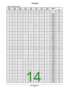
NCP5392P
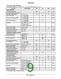
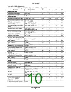
ELECTRICAL CHARACTERISTICS
(Unless otherwise stated: 0°C < T < 85°C; 4.75 V < V < 5.25 V; All DAC Codes; C
= 0.1 mF)
A
CC
VCC
Parameter
Test Conditions
Min
Typ
Max
Unit
VDROOP AMPLIFIER
Output source current (Note 3)
Output sink current (Note 3)
CSSUM AMPLIFIER
V
= 3.0 V
4
1
-
-
-
-
mA
mA
out
V
out
= 1.0 V
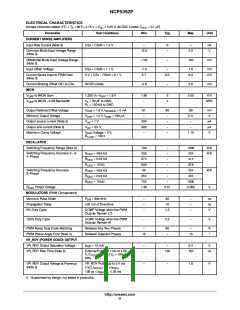
Current Sense Input to CSSUM Gain
-60 mV < CS < 60 mV
C = 10 pF to GND,
R = 10 kW to GND
-4.00
-
-3.88
4
-3.76
-
V/V
Current Sense Input to CSSUM -3 dB
Bandwidth
MHz
L
L
Current Sense Input to CSSUM
Output Slew Rate
DV = 25 mV, CL = 10 pF to
in
GND, Load = 1 k to 1.3 V
-
-15
3.0
-
4
-
-
-
-
+15
-
V/s
mV
V
Current Summing Amp Output Offset
Voltage
CSx – CSNx = 0, CSx = 1.1 V
Maximum CSSUM Output Voltage
CSx – CSxN = -0.15 V
(All Phases) I
= 1 mA
SOURCE
Minimum CSSUM Output Voltage
CSx – CSxN = 0.066 V
(All Phases) I = 1 mA
0.3
V
SINK
Output source current (Note 3)
Output sink current (Note 3)
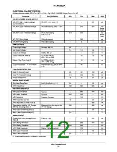
PSI (Power Saving Control, Active Low)
Enable High Input Leakage Current
Upper Threshold
V
= 3.0 V
= 0.3 V
1
1
-
-
-
-
mA
mA
out
V
out
External 1 K Pullup to 3.3 V
-
-
-
1.0
770
-
mA
mV
mV
mV
V
V
V
650
550
100
UPPER
LOWER
UPPER
Lower Threshold
450
-
Hysteresis
- V
-
LOWER
APSI_EN (AUTO PSI Function Enable, Active High)
Enable High Input Leakage Current
Upper Threshold
External 1k Pullup to 3.3 V
-
-
-
1.0
770
-
mA
mV
mV
mV
V
V
V
650
550
100
UPPER
LOWER
UPPER
Lower Threshold
450
-
Hysteresis
- V
-
LOWER
PH_PSI (PSI Phase Selection)
Enable High Input Leakage Current
Upper Threshold
External 1k Pullup to 3.3 V
-
-
-
-
-
1.0
0.7
-
mA
V
V
UPPER
LOWER
CC
CC
Lower Threshold
V
0.3
V
DRVON
Output High Voltage
Sourcing Current for Output High
Output Low Voltage
Sinking Current for Output Low
Delay Time
Sourcing 500 mA
= 5 V
3.0
-
-
2.5
-
-
4.0
0.7
-
V
mA
V
V
CC
Sinking 500 mA
-
2.5
-
-
mA
ns
Propagation Delay from EN Low
to DRVON
10
-
Rise Time
C (PCB) = 20 pF, DV = 10% to
o
-
-
130
10
-
-
ns
ns
L
90%
Fall Time
C (PCB) = 20 pF, DV = 10% to
L o
90%
Internal Pulldown Resistance
35
-
70
-
140
2.0
kW
V Voltage when DRVON
CC
Output Valid
V
3. Guaranteed by design, not tested in production.
http://onsemi.com
10

 ONSEMI [ ONSEMI ]