NCP5392P
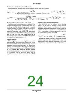
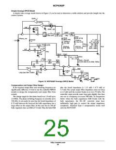
Simple Average SPICE Model
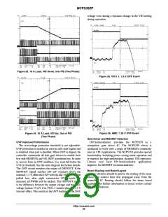
A simple state average model shown in Figure 13 can be used to determine a stable solution and provide insight into the
control system.
GAIN = 1
{-2/3*4}
E1
+
+
-
-
Voff
E
GAIN = {6}
V3
12V
0
0
L
LBRD
100p
RBRD
0.75m
DCR
{0.6E-3/4}
2
1
{185e-9/4}
1
2
0
12
CCer
{22e-6*18}
CBulk
{560e-6*6}
VRamp_min
I1 = 50
I2 = 110
TD = 100u
RSUM
1k
1.3V
ESRCer
{1.5e-3/18}
I1
ESRBulk
{7e-3/6}
TR = 50n
0Aac
0Adc
2
2
22p
CDFB
Vdrp
RDFB
2k
TF = 50n
PW = 100u
PER = 200u
ESLCer
{1.5e-9/18}
Vout
ESLBulk
{3.5e-9/6}
1E3
R8
1k
Voff
1
1
C5
10.6p
RDAC CDAC
0
0
VDAC
50
12n
DC = 1.2V
AC = 0
R12
5.11k
CFB1
680P
CH
RFB1
69.8
TRAN = PULSE
(0 0.05 400u 5u 5u 500u 1000u)
22p
RFB
RF
2.2k
CF
1.8n
R6
0
1k
Voff
1E3
R11
1k
Vdrp
Voffset
1.3V
1k
C4
10.6p
R10
2k
Unity Gain BW=15MHz
1E3
0
0
R9
C6
0
Voff
IMON
1k 10.6p
Figure 13. NCP5392P Average SPICE Model
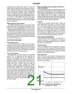
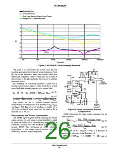
Compensation and Output Filter Design
If the required output filter and switching frequency are
significantly different, it's best to use the available PSPICE
models to design the compensation and output filter from
scratch.
plus the board impedance is 1.15 mW + 0.75 mW or
1.9 mW. The actual output filter impedance does not drop
to 1.0 mW until the ceramic breaks in at over 375 kHz. The
controller must provide some loop gain slightly less than
one out to a frequency in excess 300 kHz. At frequencies
below where the bulk capacitance ESR breaks with the
bulk capacitance, the DC-DC converter must have
sufficiently high gain to control the output impedance
completely. Standard Type-3 compensation works well
with the NCP5392P.
The design target for this demo board was 1.0 mW up to
2.0 MHz. The phase switching frequency is currently set to
330 kHz. It can easily be seen that the board impedance of
0.75 mW between the load and the bulk capacitance has a
large effect on the output filter. In this case the six 560 mF
bulk capacitors have an ESR of 7.0 mW. Thus the bulk ESR
http://onsemi.com
25

 ONSEMI [ ONSEMI ]