NCP5392P
Output Overvoltage and Undervoltage Protection and
Power Good Monitor
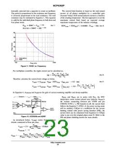
connected from the ROSC pin to ground. The user will
usually form this resistance from two resistors in order to
create a voltage divider that uses the ROSC output voltage
as the reference for creating the current limit setpoint
voltage. The oscillator frequency range is 100ꢁkHz per
phase to 1.0ꢁMHz per phase. The oscillator generates up to
4 symmetrical triangle waveforms with amplitude between
1.3ꢁV and 2.3ꢁV. The triangle waves have a phase delay
between them such that for 2-, 3- and 4-phase operation
the PWM outputs are separated by 180, 120, and 90 angular
degrees, respectively.
An output voltage monitor is incorporated. During normal
operation, if the output voltage is 180ꢁmV (typical) over the
DAC voltage, the VR_RDY goes low, the DRVON signal
remains high, the PWM outputs are set low. The outputs will
remain disabled until the V
voltage is removed and
CC
reapplied. During normal operation, if the output voltage falls
more than 350ꢁmV below the DAC setting, the VR_RDY pin
will be set low until the output voltage rises.
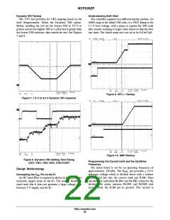
Soft-Start
There are two possible soft-start modes: AMD and
from 0 V directly
PWM Comparators with Hysteresis
VR11. AMD mode simply ramps V
to the DAC setting at a fixed rate. The VR11 mode ramps
to 1.1ꢁV boot voltage at a fixed rate of 0.8ꢁmV/mS,
core
Four PWM comparators receive an error signal at their
noninverting input. Each comparator receives one of the
triangle waves at its inverting output. The output of each
comparator generates the PWM outputs G1, G2, G3, and G4.
During steady state operation, the duty cycle will center
on the valley of the triangle waveform, with steady state
V
core
pauses at 1.1ꢁV for around 500ꢁmS, reads the VID pins to
determine the DAC setting. Then ramps V to the final
core
DAC setting at the Dynamic VID slew rate of up to
12.5ꢁmV/mS. Typical AMD and VR11 soft-start sequences
are shown in the following graphs (Figure 9 and 10).
duty cycle calculated by V /V . During a transient event,
out in
both high and low comparator output transitions shift phase
to the points where the error signal intersects the down and
up ramp of the triangle wave.
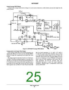
APPLICATION INFORMATION
The NCP5392P demo board for the NCP5392P is
available by request. It is configured as a four phase
solution with decoupling designed to provide a 1ꢁmW load
line under a 100ꢁA step load.
PROTECTION FEATURES
Undervoltage Lockout
An undervoltage lockout (UVLO) senses the V input.
CC
Startup Procedure
During power-up, the input voltage to the controller is
monitored, and the PWM outputs and the soft-start circuit
are disabled until the input voltage exceeds the threshold
voltage of the UVLO comparator. The UVLO comparator
incorporates hysteresis to avoid chattering.
Start by installing the test tool software. It is best to
power the test tool from a separate ATX power supply. The
test tool should be set to a valid VID code of 0.5ꢁV or above
in order for the controller to start. Consult the VTT help
manual for more detailed instruction.
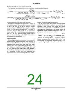
Overcurrent Shutdown
Step Load Testing
A programmable overcurrent function is incorporated
within the IC. A comparator and latch make up this
function. The inverting input of the comparator is
connected to the ILIM pin. The voltage at this pin sets the
maximum output current the converter can produce. The
ROSC pin provides a convenient and accurate reference
voltage from which a resistor divider can create the
overcurrent setpoint voltage. Although not actually
disabled, tying the ILIM pin directly to the ROSC pin sets
the limit above useful levels - effectively disabling
overcurrent shutdown. The comparator noninverting input
is the summed current information from the VDRP minus
offset voltage. The overcurrent latch is set when the current
information exceeds the voltage at the ILIM pin. The
outputs are pulled low, and the soft-start is pulled low. The
The VTT tool is used to generate the d /d step load.
t
i
Select the dynamic loading option in the VTT test tool
software. Set the desired step load size, frequency, duty,
and slew rate. See Figure 6.
outputs will remain disabled until the V
voltage is
CC
removed and re-applied, or the ENABLE input is brought
low and then high.
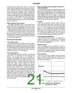
Figure 6. Typical Load Step Response
(full load, 35 A - 100 A)
http://onsemi.com
21

 ONSEMI [ ONSEMI ]