NCP3170
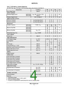
Table 4. ELECTRICAL CHARACTERISTICS
(T = 25°C, V = V = 12 V, V = 3.3 V for min/max values unless otherwise noted (Note 7))
A
IN
EN
OUT
Characteristic
Conditions
Min
Typ
Max
Unit
Input Voltage Range
(Note 5)
4.5
−
18
V
SUPPLY CURRENT
Quiescent Supply Current
NCP3170A
NCP3170B
V
IN
= EN = 12 V V = 0.8 V
−
−
1.7
1.7
2.0
2.0
mA
FB
(Note 5)
Shutdown Supply Current
UNDER VOLTAGE LOCKOUT
VIN UVLO Threshold
VIN UVLO Threshold
MODULATOR
EN = 0 V (Note 5)
−
13
17
mA
V
Rising Edge (Note 5)
Falling Edge (Note 5)
−
−
4.41
4.13
−
−
V
V
IN
V
IN
Oscillator Frequency
NCP3170A
NCP3170B
Enable = V
450
900
500
550
kHz
%
IN
1000
1100
Maximum Duty Ratio
Minimum Duty Ratio
NCP3170A
NCP3170B
91
90
−
−
96
96
NCP3170A
NCP3170B
V
IN
= 12 V
6.0
4.0
−
−
11
11.5
%
VIN Soft Start Ramp Time
OVER CURRENT
Current Limit
V
FB
= VCOMP
3.5
4.6
6.0
6.0
ms
(Note 4)
4.0
−
A
PWM COMPENSATION
VFB Feedback Voltage
Line Regulation
GM
T = 25°C
0.792
−
0.8
1
0.808
V
%
A
(Note 4)
−
−
−
201
55
mS
dB
MHz
nA
mA
mA
AOL DC gain
(Note 4)
(Note 4)
(Note 4)
40
2.0
−
−
Unity Gain BW (C
= 10 pF)
−
−
OUT
Input Bias Current (Current Out of FB IB Pin)
IEAOP Output Source Current
IEAOM Output Sink Current
ENABLE
−
286
−
V
FB
V
FB
= 0 V
= 2 V
−
20.1
21.3
−
−
Enable Threshold
(Note 5)
−
1.41
−
V
POWER GOOD
Power Good High On Threshold
Power Good High Off Threshold
Power Good Low On Threshold
Power Good Low Off Threshold
Over Voltage Protection Threshold
Power Good Low Voltage
PWM OUTPUT STAGE
−
−
−
−
−
−
875
859
−
−
−
−
−
−
mV
mV
mV
mV
mV
V
712
728
998
V
IN
= 12 V, IPG = 500 mA
0.195
High-Side Switch On-Resistance
V
= 12 V
= 4.5 V
−
−
90
130
150
mW
mW
IN
IN
V
100
Low-Side Switch On-Resistance
V
= 12 V
= 4.5 V
−
−
25
29
35
39
IN
IN
V
THERMAL SHUTDOWN
Thermal Shutdown
Hysteresis
(Notes 4 and 6)
−
−
164
43
−
−
°C
°C
4. Guaranteed by design
5. Ambient temperature range of −40°C to +85°C.
6. This is not a protection feature.
7. The device is not guaranteed to operate beyond the maximum operating ratings.
http://onsemi.com
4

 ONSEMI [ ONSEMI ]