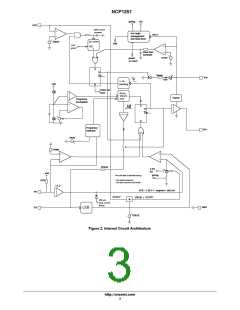
NCP1251
ELECTRICAL CHARACTERISTICS
(For typical values T = 25°C, for min/max values T = −40°C to +125°C, Max T = 150°C, V = 12 V unless otherwise noted)
J
J
J
CC
Symbol
Rating
Pin
Min
Typ
Max
Unit
SUPPLY SECTION
VCC
V
V
increasing level at which driving pulses are authorized
decreasing level at which driving pulses are stopped
5
5
5
5
5
5
5
5
5
5
16
8.2
6.0
18
20
V
V
ON
(min)
CC
CC
VCC
8.8
9.4
VCC
Hysteresis VCC − VCC
(min)
V
HYST
ZENER
ON
V
Clamped V when latched off / burst mode activation @ I = 500 mA
7.0
V
CC
CC
ICC1
ICC2
Start−up current
15
2.2
3.0
2.5
4.0
mA
mA
mA
mA
mA
mA
Internal IC consumption with I = 50 mA, F
= 65 kHz and C = 0 nF
1.4
2.1
1.7
3.1
550
FB
SW
SW
SW
SW
L
ICC3
Internal IC consumption with I = 50 mA, F
= 65 kHz and C = 1 nF
L
FB
ICC2
Internal IC consumption with I = 50 mA, F
= 100 kHz and C = 0 nF
L
FB
ICC3
Internal IC consumption with I = 50 mA, F
= 100 kHz and C = 1 nF
L
FB
ICCstby
Internal IC consumption while in skip cycle (V = 12 V, driving a typical 6 A/600 V
MOSFET)
CC
ICC
Current flowing into V pin that keeps the controller latched (Note 4)
5
5
mA
kW
LATCH
CC
T = −40°C to +125°C
40
32
J
T = 0°C to +125°C
J
R
Current−limit resistor in series with the latch SCR
DRIVE OUTPUT
Output voltage rise−time @ C = 1 nF, 10−90% of output signal
4.0
lim
T
r
6
6
6
6
6
6
6
6
40
30
ns
ns
W
L
T
f
Output voltage fall−time @ C = 1 nF, 10−90% of output signal
L
R
Source resistance
Sink resistance
13
OH
R
6.0
300
500
W
OL
I
Peak source current, V = 0 V – (Note 5)
mA
mA
V
source
GS
I
Peak sink current, V = 12 V – (Note 5)
GS
sink
V
DRV pin level at V close to VCC with a 33 kW resistor to GND
(min)
8.0
10
DRVlow
CC
V
DRV pin level at V = 28 V – DRV unloaded
12
14
V
DRVhigh
CC
CURRENT COMPARATOR
Input Bias Current @ 0.8 V input level on pin 4
Maximum internal current setpoint – T = 25°C – pin 3 grounded
I
4
4
4
3
3
4
4
−
3
3
3
3
0.02
0.8
0.8
357
250
100
300
4
mA
V
IB
V
V
0.744
0.72
0.856
0.88
Limit1
Limit2
J
Maximum internal current setpoint – T = −40°C to 125°C – pin 3 grounded
V
J
V
fold
Default internal voltage set point for frequency foldback trip point – 45% of V
mV
mV
ns
ns
ms
%
limit
V
freeze
Internal peak current setpoint freeze ([31% of V
)
limit
T
Propagation delay from current detection to gate off−state
Leading Edge Blanking Duration
150
DEL
LEB
T
TSS
Internal soft−start duration activated upon startup, auto−recovery
Setpoint decrease for pin 3 biased to –250 mV – (Note 6)
IOPPo
IOOPv
IOOPv
IOPPs
31.3
0.55
0.55
0
Voltage setpoint for pin 3 biased to −250 mV – (Note 6), T = 25°C
0.51
0.50
0.60
0.62
V
J
Voltage setpoint for pin 3 biased to −250 mV – (Note 6), T = −40°C to 125°C
V
J
Setpoint decrease for pin 3 grounded
%
4. For design robustness, we recommend to inject 60 mA as a minimum at the lowest input line voltage.
5. Guaranteed by design
6. See characterization table for linearity over negative bias voltage
7. A 1 MW resistor is connected from pin 3 to the ground for the measurement.
http://onsemi.com
5

 ONSEMI [ ONSEMI ]