NCP1251
Vbulk
Vout
.
.
OVP
OPP
.
NCP1251
1
2
3
6
5
4
ramp
comp.
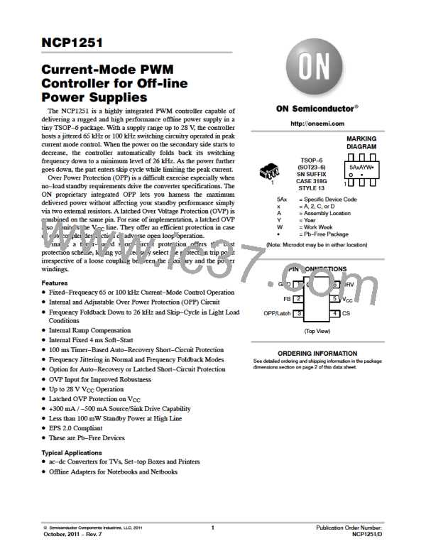
Figure 1. Typical Application Example
Pin N5
1
2
3
Pin Name
GND
Function
−
Pin Description
The controller ground.
FB
Feedback pin
Hooking an optocoupler collector to this pin will allow regulation.
A resistive divider from the auxiliary winding to this pin sets the OPP
OPP/OVP
Adjust the Over Power Protection
Latches off the part
compensation level. When brought above 3 V, the part is fully latched off.
4
5
CS
Current sense + ramp
compensation
This pin monitors the primary peak current but also offers a means to
introduce ramp compensation.
V
CC
Supplies the controller
This pin is connected to an external auxiliary voltage and supplies the
controller. When the V exceeds a certain level, the part permanently
CC
latches off.
6
DRV
Driver output
The driver’s output to an external MOSFET gate.
OPTIONS
Controller
Frequency
65 kHz
OCP Latched
OCP Auto−Recovery
NCP1251ASN65T1G
NCP1251BSN65T1G
NCP1251ASN100T1G
NCP1251BSN100T1G
Yes
No
No
Yes
No
65 kHz
100 kHz
100 kHz
Yes
No
Yes
ORDERING INFORMATION
†
Device
Package Marking
OCP Protection
Latch
Switching Frequency
65 kHz
Package
Shipping
NCP1251ASN65T1G
NCP1251BSN65T1G
NCP1251ASN100T1G
NCP1251BSN100T1G
5AA
5A2
5AC
5AD
Autorecovery
Latch
65 kHz
TSOP−6
(Pb−Free)
3000 /
Tape & Reel
100 kHz
Autorecovery
100 kHz
†For information on tape and reel specifications, including part orientation and tape sizes, please refer to our Tape and Reel Packaging
Specifications Brochure, BRD8011/D.
http://onsemi.com
2

 ONSEMI [ ONSEMI ]