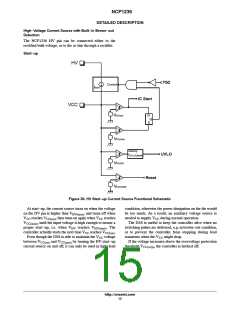
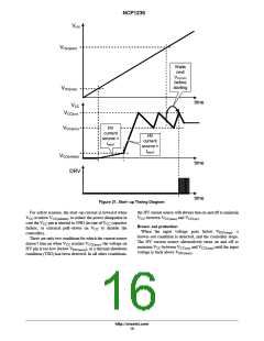
NCP1236
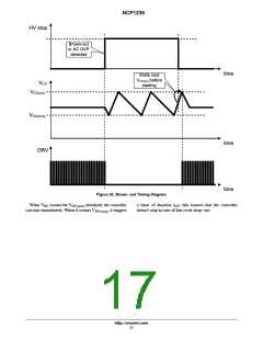
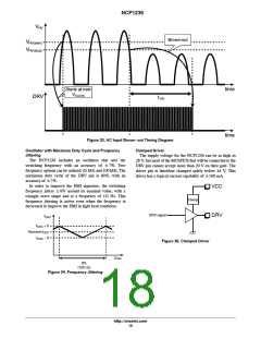
VHV
Brown-out
VHV(start)
VHV(stop)
time
Starts at next
VCC(ON)
DRV
tHV
time
Figure 33. AC Input Brown−out Timing Diagram
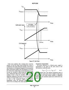
Oscillator with Maximum Duty Cycle and Frequency
Jittering
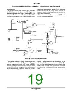
Clamped Driver
The supply voltage for the NCP1236 can be as high as
28 V, but most of the MOSFETs that will be connected to the
DRV pin cannot accept more than 20 V on their gate. The
driver pin is therefore clamped safely below 16 V. This
driver has a typical current capability of $500 mA.
The NCP1236 includes an oscillator that sets the
switching frequency with an accuracy of $7%. Two
frequency options can be ordered: 65 kHz and 100 kHz. The
maximum duty cycle of the DRV pin is 80%, with an
accuracy of $7%.
In order to improve the EMI signature, the switching
frequency jitters $6% around its nominal value, with a
triangle−wave shape and at a frequency of 125 Hz. This
frequency jittering is active even when the frequency is
decreased to improve the EMI in light load condition.
VCC
Clamp
DRV signal
DRV
f
OSC
f
+ 6
OSC
Nominal f
OSC
f
− 6
OSC
Figure 35. Clamped Driver
Time
8%
(125 Hz)
Figure 34. Frequency Jittering
http://onsemi.com
18

 ONSEMI [ ONSEMI ]