MC74HC4538A
PIN DESCRIPTIONS
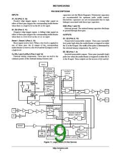
INPUTS
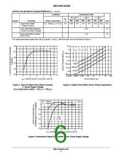
capacitors (see the Block Diagram). Polystyrene capacitors
are recommended for optimum pulse width control.
Electrolytic capacitors are not recommended due to high
leakages associated with these type capacitors.
A1, A2 (Pins 4, 12)
Positive−edge trigger inputs. A rising−edge signal on
either of these pins triggers the corresponding multivibrator
when there is a high level on the B1 or B2 input.
GND (Pins 1 and 15)
External ground. The external timing capacitors discharge
to ground through these pins.
B1, B2 (Pins 5, 11)
Negative−edge trigger inputs. A falling−edge signal on
either of these pins triggers the corresponding multivibrator
when there is a low level on the A1 or A2 input.
OUTPUTS
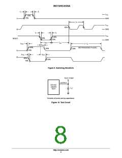
Q1, Q2 (Pins 6, 10)
Reset 1, Reset 2 (Pins 3, 13)
Noninverted monostable outputs. These pins (normally
low) pulse high when the multivibrator is triggered at either
the A or the B input. The width of the pulse is determined by
Reset inputs (active low). When a low level is applied to
one of these pins, the Q output of the corresponding
multivibrator is reset to a low level and the Q output is set to
a high level.
the external timing components, R and C .
X
X
Q1, Q2 (Pins 7, 9)
CX1/RX1 and CX2/RX2 (Pins 2 and 14)
External timing components. These pins are tied to the
common points of the external timing resistors and
Inverted monostable outputs. These pins (normally high)
pulse low when the multivibrator is triggered at either the A
or the B input. These outputs are the inverse of Q1 and Q2.
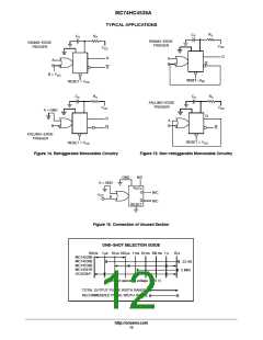
RxCx
UPPER
REFERENCE
CIRCUIT
OUTPUT
LATCH
−
+
V
CC
V ,
re
UPPER
LOWER
REFERENCE
CIRCUIT
M1
V
CC
2 kW
−
+
M2
Q
Q
V ,
LOWER
re
M3
TRIGGER
CONTROL CIRCUIT
A
B
C
Q
TRIGGER CONTROL
RESET CIRCUIT
CB
R
RESET
POWER
ON
RESET
RESET LATCH
Figure 11. Logic Detail (1/2 the Device)
http://onsemi.com
9

 ONSEMI [ ONSEMI ]