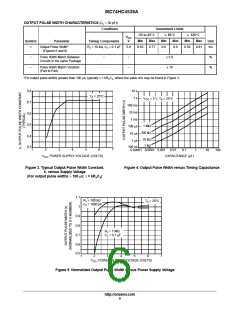
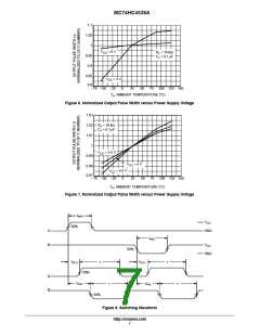
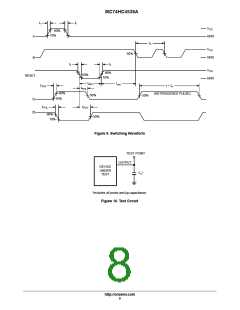
MC74HC4538A
CIRCUIT OPERATION
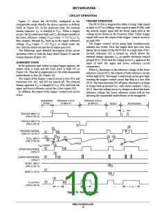
TRIGGER OPERATION
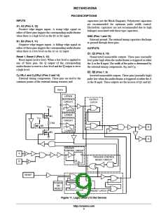
Figure 12 shows the HC4538A configured in the
retriggerable mode. Briefly, the device operates as follows
(refer to Figure 10): In the quiescent state, the external
The HC4538A is triggered by either a rising−edge signal
at input A (#7) or a falling−edge signal at input B (#8), with
the unused trigger input and the Reset input held at the
voltage levels shown in the Function Table. Either trigger
signal will cause the output of the trigger−control circuit to
go high (#9).
timing capacitor, C , is charged to V . When a trigger
x
CC
occurs, the Q output goes high and C discharges quickly to
x
the lower reference voltage (V Lower [ 1/3 V ). C
ref
CC
x
then charges, through R , back up to the upper reference
x
The trigger−control circuit going high simultaneously
initiates two events. First, the output latch goes low, thus
taking the Q output of the HC4538A to a high state (#10).
Second, transistor M3 is turned on, which allows the
voltage (V Upper [ 2/3 V ), at which point the
ref
CC
one−shot has timed out and the Q output goes low.
The following, more detailed description of the circuit
operation refers to both the logic detail (Figure 9) and the
timing diagram (Figure 10).
external timing capacitor, C , to rapidly discharge toward
x
ground (#11). (Note that the voltage across C appears at the
input of both the upper and lower reference circuit
comparator).
x
QUIESCENT STATE
In the quiescent state, before an input trigger appears, the
output latch is high and the reset latch is high (#1 in
Figure 10). Thus the Q output (pin 6 or 10) of the monostable
multivibrator is low (#2, Figure 10).
The output of the trigger−control circuit is low (#3), and
transistors M1, M2, and M3 are turned off. The external
When C discharges to the reference voltage of the lower
x
reference circuit (#12), the outputs of both reference circuits
will be high (#13). The trigger−control reset circuit goes high,
resetting the trigger−control circuit flip−flop to a low state
(#14). This turns transistor M3 off again, allowing C to begin
x
timing capacitor, C , is charged to V (#4), and both the
x
CC
to charge back up toward V , with a time constant t = R C
CC
x x
upper and lower reference circuit has a low output (#5).
In addition, the output of the trigger−control reset circuit
is low.
(#15). Once the voltage across C charges to above the lower
x
reference voltage, the lower reference circuit will go low
allowing the monostable multivibrator to be retriggered.
QUIESCENT
STATE
TRIGGER CYCLE
(A INPUT)
TRIGGER CYCLE
(B INPUT)
RESET
RETRIGGER
t
rr
7
TRIGGER INPUT A
(PIN 4 OR 12)
TRIGGER INPUT B
(PIN 5 OR 11)
8
24
9
TRIGGER-CONTROL
CIRCUIT OUTPUT
3
14
11
4
21
23
15
17
18
R /C INPUT
X
X
12
(PIN 2 OR 14)
V
ref
UPPER
25
13
V
ref
LOWER
5
UPPER REFERENCE
CIRCUIT
13
6
16
LOWER REFERENCE
CIRCUIT
RESET INPUT
(PIN 3 OR 13)
20
1
RESET LATCH
22
10
2
19
Q OUTPUT
(PIN 6 OR 10)
τ
τ
τ + t
rr
Figure 12. Timing Diagram
http://onsemi.com
10

 ONSEMI [ ONSEMI ]