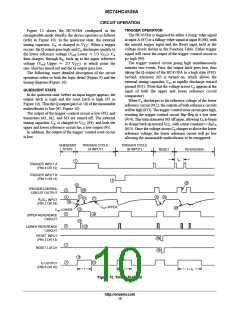
MC74HC4538A
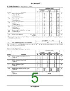
OUTPUT PULSE WIDTH CHARACTERISTICS (C = 50 pF)t
L
Conditions
Guaranteed Limits
–55 to 25_C
v 85_C
v 125_C
V
V
CC
Min
Max
Min
Max
Min
Max
Symbol
Parameter
Timing Components
Unit
τ
Output Pulse Width*
(Figures 6 and 8)
R = 10 kW, C = 0.1 mF
5.0
0.63
0.77
0.6
0.8
0.59
0.81
ms
x
x
−
−
Pulse Width Match Between
Circuits in the same Package
−
−
−
−
5.0
%
%
Pulse Width Match Variation
(Part to Part)
10
*For output pulse widths greater than 100 ms, typically τ = kR C , where the value of k may be found in Figure 3.
x
x
0.8
0.7
0.6
0.5
0.4
0.3
10 s
1 s
T = 25°C
A
V
= 5 V, T = 25°C
A
CC
100 ms
10 ms
1 ms
1 MW
100 ms
10 ms
100 kW
10 kW
1 kW
1 ms
100 ns
1
2
3
4
5
6
7
0.00001 0.0001 0.001 0.01
0.1
1
10
100
V
, POWER SUPPLY VOLTAGE (VOLTS)
CC
CAPACITANCE (mF)
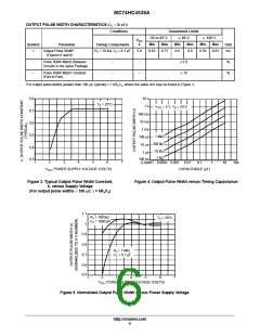
Figure 3. Typical Output Pulse Width Constant,
k, versus Supply Voltage
Figure 4. Output Pulse Width versus Timing Capacitance
(For output pulse widths > 100 ms: τ = kRxCx)
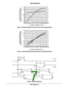
1.1
R = 100 kW
x
T = 25°C
A
C = 1000 pF
x
1
0.9
0.8
0.7
R = 1 MW
C = 0.1 mF
x
x
0.6
0.5
1
2
3
4
5
6
7
V
, POWER SUPPLY VOLTAGE (VOLTS)
CC
Figure 5. Normalized Output Pulse Width versus Power Supply Voltage
http://onsemi.com
6

 ONSEMI [ ONSEMI ]