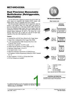
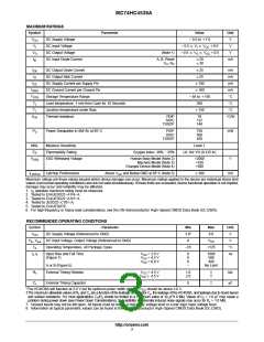
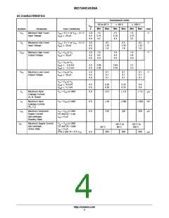
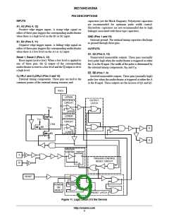
MC74HC4538A
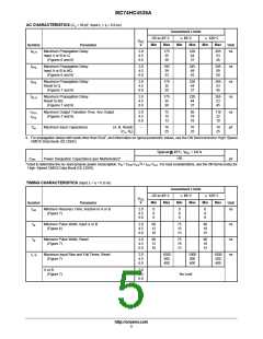
AC CHARACTERISTICS (C = 50 pF, Input t = t = 6.0 ns)
L
r
f
Guaranteed Limits
–55 to 25_C
v 85_C
v 125_C
V
V
CC
Min
Max
Min
Max
Min
Max
Symbol
Parameter
Unit
t
t
t
t
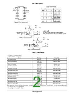
Maximum Propagation Delay
Input A or B to Q
(Figures 6 and 8)
2.0
4.5
6.0
175
35
30
220
44
37
265
53
45
ns
PLH
PHL
PHL
PLH
Maximum Propagation Delay
Input A or B to NQ
(Figures 6 and 8)
2.0
4.5
6.0
195
39
33
245
49
42
295
59
50
ns
ns
ns
ns
pF
Maximum Propagation Delay
Reset to Q
(Figures 7 and 8)
2.0
4.5
6.0
175
35
30
220
44
37
265
53
45
Maximum Propagation Delay
Reset to NQ
(Figures 7 and 8)
2.0
4.5
6.0
175
35
30
220
44
37
265
53
45
t
Maximum Output Transition Time, Any Output
(Figures 7 and 8)
2.0
4.5
6.0
75
15
13
95
19
16
110
22
19
TLH,
t
THL
C
Maximum Input Capacitance
(A. B, Reset)
(C , R )
−
10
25
10
25
10
25
in
x
x
9. For propagation delays with loads other than 50 pF, and information on typical parametric values, see the ON Semiconductor High−Speed
CMOS Data Book (DL129/D).
Typical @ 25°C, V = 5.0 V
CC
150
C
PD
Power Dissipation Capacitance (per Multivibrator)*
pF
2
*Used to determine the no−load dynamic power consumption: P = C
V
f + I V . For load considerations, see the ON Semiconductor
CC CC
D
PD CC
High−Speed CMOS Data Book (DL129/D).
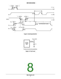
TIMING CHARACTERISTICS (Input t = t = 6.0 ns)
r
f
Guaranteed Limits
–55 to 25_C
v 85_C
v 125_C
V
V
CC
Min
Max
Min
Max
Min
Max
Symbol
Parameter
Unit
t
Minimum Recovery Time, Inactive to A or B
(Figure 7)
2.0
4.5
6.0
0
0
0
0
0
0
0
0
0
ns
rec
t
t
Minimum Pulse Width, Input A or B
(Figure 6)
2.0
4.5
6.0
60
12
10
75
15
13
90
18
15
ns
ns
ns
w
w
Minimum Pulse Width, Reset
(Figure 7)
2.0
4.5
6.0
60
12
10
75
15
13
90
18
15
t , t
r
Maximum Input Rise and Fall Times, Reset
(Figure 7)
2.0
4.5
6.0
1000
500
400
1000
500
400
1000
500
400
f
A or B
(Figure 7)
2.0
4.5
6.0
No Limit
http://onsemi.com
5

 ONSEMI [ ONSEMI ]