MC74HC4538A
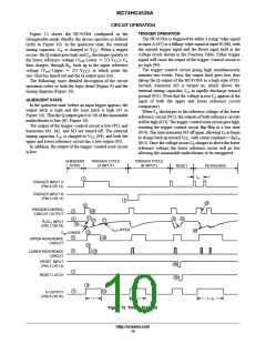
When C charges up to the reference voltage of the upper
reference circuit (#17), the output of the upper reference
occurs, the output of the reset latch goes low (#22), turning
on transistor M1. Thus C is allowed to quickly charge up to
x
x
circuit goes low (#18). This causes the output latch to toggle,
taking the Q output of the HC4538A to a low state (#19), and
completing the time−out cycle.
V
(#23) to await the next trigger signal.
On power up of the HC4538A the power−on reset circuit
CC
will be high causing a reset condition. This will prevent the
trigger−control circuit from accepting a trigger input during
this state. The HC4538A’s Q outputs are low and the Q not
outputs are high.
POWER−DOWN CONSIDERATIONS
Large values of C may cause problems when powering
x
down the HC4538A because of the amount of energy stored
in the capacitor. When a system containing this device is
RETRIGGER OPERATION
powered down, the capacitor may discharge from V
through the input protection diodes at pin 2 or pin 14.
Current through the protection diodes must be limited to 30
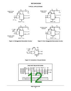
When used in the retriggerable mode (Figure 12), the
HC4538A may be retriggered during timing out of the
output pulse at any time after the trigger−control circuit
CC
mA; therefore, the turn−off time of the V power supply
flip−flop has been reset (#24), and the voltage across C is
CC
x
must not be faster than t = V ꢀ C /(30 mA). For example,
above the lower reference voltage. As long as the C voltage
CC
x
x
if V = 5.0 V and C = 15 mF, the V supply must turn off
is below the lower reference voltage, the reset of the
flip−flop is high, disabling any trigger pulse. This prevents
M3 from turning on during this period resulting in an output
pulse width that is predictable.
CC
x
CC
no faster than t = (5.0 V)ꢀ (15 mF)/30 mA = 2.5 ms. This is
usually not a problem because power supplies are heavily
filtered and cannot discharge at this rate.
The amount of undershoot voltage on R C during the
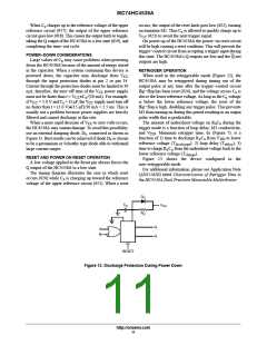
When a more rapid decrease of V to zero volts occurs,
x
x
CC
the HC4538A may sustain damage. To avoid this possibility,
trigger mode is a function of loop delay, M3 conductivity,
and V . Minimum retrigger time, trr (Figure 7), is a
use an external damping diode, D , connected as shown in
DD
x
function of 1) time to discharge R C from V to lower
Figure 11. Best results can be achieved if diode D is chosen
x
x
DD
x
reference voltage (T
); 2) loop delay (T
); 3)
to be a germanium or Schottky type diode able to withstand
large current surges.
discharge
delay
time to charge R C from the undershoot voltage back to the
x
x
lower reference voltage (T
Figure 13 shows the device configured in the
non−retriggerable mode.
For additional information, please see Application Note
(AN1558/D) titled Characterization of Retrigger Time in
the HC4538A Dual Precision Monostable Multivibrator.
).
charge
RESET AND POWER ON RESET OPERATION
A low voltage applied to the Reset pin always forces the
Q output of the HC4538A to a low state.
The timing diagram illustrates the case in which reset
occurs (#20) while C is charging up toward the reference
x
voltage of the upper reference circuit (#21). When a reset
D
X
X
C
X
V
CC
R
Q
Q
A
B
RESET
Figure 13. Discharge Protection During Power Down
http://onsemi.com
11

 ONSEMI [ ONSEMI ]