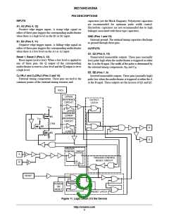
MC74HC4538A
MAXIMUM RATINGS
Symbol
Parameter
Value
Unit
V
V
DC Supply Voltage
DC Input Voltage
*0.5 to )7.0
CC
V
*0.5 v V v V )0.5
V
I
O
I
CC
V
DC Output Voltage
DC Input Diode Current
(Note 1)
*0.5 v V v V )0.5
V
O
CC
I
A, B, Reset
$20
$30
mA
IK
C , R
X
X
I
I
DC Output Diode Current
$25
$25
mA
mA
mA
mA
_C
OK
I
DC Output Sink Current
O
DC Supply Current per Supply Pin
DC Ground Current per Ground Pin
Storage Temperature Range
$100
$100
CC
I
GND
T
*65 to )150
260
STG
T
Lead temperature, 1 mm from Case for 10 Seconds
Junction temperature under Bias
Thermal resistance
_C
L
T
)150
_C
_C/W
J
q
PDIP
SOIC
TSSOP
78
112
148
JA
P
Power Dissipation in Still Air at 85_C
PDIP
SOIC
TSSOP
750
500
450
mW
D
MSL
Moisture Sensitivity
Flammability Rating
ESD Withstand Voltage
Level 1
F
Oxygen Index: 30% − 35%
UL−94−VO (0.125 in)
R
V
Human Body Model (Note 2)
Machine Model (Note 3)
Charged Device Model (Note 4)
>2000
>100
>500
V
ESD
I
Latchup Performance
Above V and Below GND at 85_C (Note 5)
$300
mA
Latchup
CC
Maximum ratings are those values beyond which device damage can occur. Maximum ratings applied to the device are individual stress limit
values (not normal operating conditions) and are not valid simultaneously. If these limits are exceeded, device functional operation is not implied,
damage may occur and reliability may be affected.
1. I absolute maximum rating must be observed.
O
2. Tested to EIA/JESD22−A114−A.
3. Tested to EIA/JESD22−A115−A.
4. Tested to JESD22−C101−A.
5. Tested to EIA/JESD78.
6. For high frequency or heavy load considerations, see the ON Semiconductor High−Speed CMOS Data Book (DL129/D).
RECOMMENDED OPERATING CONDITIONS
Symbol
Parameter
DC Supply Voltage (Referenced to GND)
Min
3.0*
0
Max
Unit
V
V
6.0
CC
V , V
in out
DC Input Voltage, Output Voltage (Referenced to GND)
Operating Temperature, All Package Types
V
V
CC
T
A
–55
+125
_C
ns
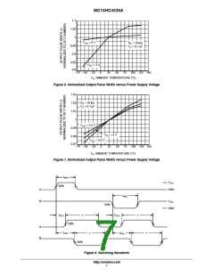
t , t
r
Input Rise and Fall Time
(Figure 7)
V
V
V
= 2.0 V
= 4.5 V
= 6.0 V
0
0
0
−
1000
500
400
f
CC
CC
CC
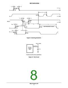
A or B (Figure 5)
No Limit
R
C
External Timing Resistor
V
< 4.5 V
≥ 4.5 V
1.0
2.0
†
†
kW
mF
x
CC
V
CC
External Timing Capacitor
0
†
x
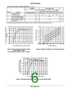
*The HC4538A will function at 2.0 V but for optimum pulse−width stability, V should be above 3.0 V.
CC
†The maximum allowable values of R and C are a function of the leakage of capacitor C , the leakage of the HC4538A, and leakage due to board layout
x
x
x
and surface resistance. For most applications, C /R should be limited to a maximum value of 10 mF/1.0 MW. Values of C > 1.0 mF may cause a
x
x
x
problem during power down (see Power Down Considerations). Susceptibility to externally induced noise signals may occur for R > 1.0 MW.
x
7. Unused inputs may not be left open. All inputs must be tied to a high−logic voltage level or a low−logic input voltage level.
8. Information on typical parametric values can be found in the ON Semiconductor High−Speed CMOS Data Book (DL129/D).
http://onsemi.com
3

 ONSEMI [ ONSEMI ]