MC54/74HC390
PIN DESCRIPTIONS
OUTPUTS
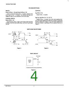
INPUTS
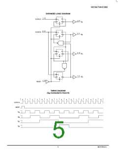
Clock A (Pins 1, 15) and Clock B (Pins 4, 15)
Q
(Pins 3, 13)
A
Clock A is the clock input to the ÷ 2 counter; Clock B is the
clock input to the ÷ 5 counter. The internal flip–flops are
toggled by high–to–low transitions of the clock input.
Output of the ÷ 2 counter.
Q , Q , Q (Pins 5, 6, 7, 9, 10, 11)
B
C
D
CONTROL INPUTS
Outputs of the ÷ 5 counter. Q is the most significant bit.
D
Reset (Pins 2, 14)
Q
is the least significant bit when the counter is connected
A
Asynchronous reset. A high at the Reset input prevents
counting, resets the internal flip–flops, and forces Q through
for BCD output as in Figure 4. Q is the least significant bit
B
when the counter is operating in the bi–quinary mode as in
Figure 5.
A
Q
low.
D
SWITCHING WAVEFORMS
t
t
f
r
t
w
V
90%
50%
10%
CC
V
CLOCK
CC
50%
RESET
10%
GND
GND
t
w
t
PHL
1/f
max
t
t
50%
PLH
PHL
Q
90%
50%
10%
Q
t
rec
V
CC
t
t
50%
TLH
THL
CLOCK
GND
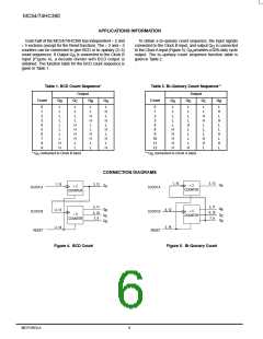
Figure 1.
Figure 2.
TEST CIRCUIT
TEST POINT
OUTPUT
DEVICE
UNDER
TEST
C *
L
* Includes all probe and jig capacitance
Figure 3.
MOTOROLA
4
High–Speed CMOS Logic Data
DL129 — Rev 6

 ONSEMI [ ONSEMI ]