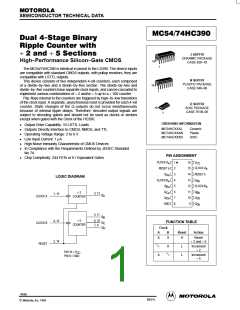
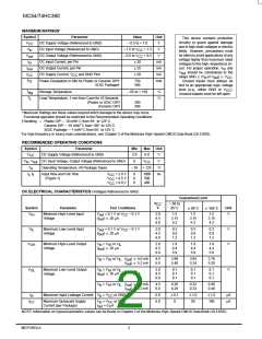
MC54/74HC390
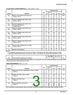
AC ELECTRICAL CHARACTERISTICS (C = 50 pF, Input t = t = 6 ns)
L
f
f
Guaranteed Limit
– 55 to
V
CC
V
25 C
Symbol
Parameter
Unit
85 C
125 C
f
Maximum Clock Frequency (50% Duty Cycle)
(Figures 1 and 3)
2.0
4.5
6.0
5.4
27
32
4.4
22
26
3.6
18
21
MHz
max
t
t
t
t
t
,
Maximum Propagation Delay, Clock A to QA
(Figures 1 and 3)
2.0
4.5
6.0
120
24
20
150
30
26
180
36
31
ns
ns
ns
ns
ns
ns
ns
pF
PLH
t
PHL
,
Maximum Propagation Delay, Clock A to QC
(QA connected to Clock B)
(Figures 1 and 3)
2.0
4.5
6.0
290
58
49
365
73
62
435
87
74
PLH
t
PHL
,
Maximum Propagation Delay, Clock B to QB
(Figures 1 and 3)
2.0
4.5
6.0
130
26
22
165
33
28
195
39
33
PLH
t
PHL
,
Maximum Propagation Delay, Clock B to QC
(Figures 1 and 3)
2.0
4.5
6.0
185
37
31
230
46
39
280
56
48
PLH
t
PHL
,
Maximum Propagation Delay, Clock B to QD
(Figures 1 and 3)
2.0
4.5
6.0
130
26
22
165
33
28
195
39
33
PLH
t
PHL
t
Maximum Propagation Delay, Reset to any Q
(Figures 2 and 3)
2.0
4.5
6.0
165
33
28
205
41
35
250
50
43
PHL
t
t
,
Maximum Output Transition Time, Any Output
(Figures 1 and 3)
2.0
4.5
6.0
75
15
13
95
19
16
110
22
19
TLH
THL
C
Maximum Input Capacitance
—
10
10
10
in
NOTES:
1. For propagation delays with loads other than 50 pF, see Chapter 2 of the Motorola High–Speed CMOS Data Book (DL129/D).
2. Information on typical parametric values can be found in Chapter 2 of the Motorola High–Speed CMOS Data Book (DL129/D).
Typical @ 25°C, V
= 5.0 V
CC
C
Power Dissipation Capacitance (Per Counter)*
pF
35
PD
2
* Used to determine the no–load dynamic power consumption: P = C
D
Motorola High–Speed CMOS Data Book (DL129/D).
V
f + I
V
. For load considerations, see Chapter 2 of the
PD CC
CC CC
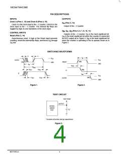
TIMING REQUIREMENTS (Input t = t = 6 ns)
r
f
Guaranteed Limit
– 55 to
V
CC
V
25 C
Symbol
Parameter
Unit
85 C
125 C
t
Minimum Recovery Time, Reset Inactive to Clock A or Clock B
(Figure 2)
2.0
4.5
6.0
50
10
9
65
13
11
75
15
13
ns
rec
t
t
Minimum Pulse Width, Clock A, Clock B
(Figure 1)
2.0
4.5
6.0
80
16
14
100
20
17
120
24
20
ns
ns
ns
w
Minimum Pulse Width, Reset
(Figure 2)
2.0
4.5
6.0
125
25
21
155
31
26
190
38
32
w
t , t
f
Maximum Input Rise and Fall Times
(Figure 1)
2.0
4.5
6.0
1000
500
400
1000
500
400
1000
500
400
f
NOTE: Information on typical parametric values can be found in Chapter 2 of the Motorola High–Speed CMOS Data Book (DL129/D).
High–Speed CMOS Logic Data
DL129 — Rev 6
3
MOTOROLA

 ONSEMI [ ONSEMI ]