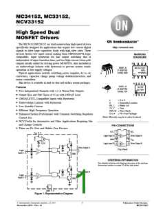
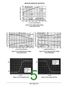
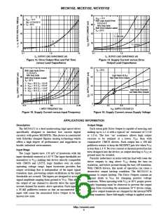
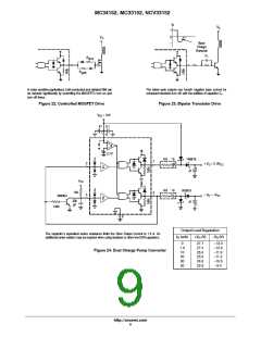
MC34152, MC33152, NCV33152
ELECTRICAL CHARACTERISTICS (V = 12 V, for typical values T = 25°C, for min/max values T is the operating ambient
CC
A
A
temperature range that applies [Note 3], unless otherwise noted.)
Characteristics
Symbol
Min
Typ
Max
Unit
LOGIC INPUTS
Input Threshold Voltage
V
Output Transition High−to−Low State
Output Transition Low−to−High State
V
V
−
0.8
1.75
1.58
2.6
−
IH
IL
Input Current
High State (V = 2.6 V)
mA
I
I
−
−
100
20
300
100
IH
IH
Low State (V = 0.8 V)
IL
IL
DRIVE OUTPUT
Output Voltage
V
Low State (I
Low State (I
Low State (I
High State (I
High State (I
High State (I
= 10 mA)
= 50 mA)
= 400 mA)
V
−
−
−
10.5
10.4
10
0.8
1.1
1.8
11.2
11.1
10.8
1.2
1.5
2.5
−
−
−
sink
sink
sink
OL
= 10 mA)
= 50 mA)
= 400 mA)
V
OH
source
source
source
Output Pull−Down Resistor
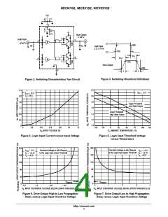
SWITCHING CHARACTERISTICS (T = 25°C)
R
PD
−
100
−
kW
A
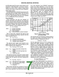
Propagation Delay (C = 1.0 nF)
ns
L
Logic Input to: Drive Output Rise (10% Input to 10% Output)
Drive Output Fall (90% Input to 90% Output)
t
t
−
−
55
40
120
120
PLH (IN/OUT)
PHL (IN/OUT)
Drive Output Rise Time (10% to 90%)
Drive Output Rise Time (10% to 90%)
C = 1.0 nF
C = 2.5 nF
L
t
−
−
14
36
30
−
ns
ns
L
r
Drive Output Fall Time (90% to 10%)
Drive Output Fall Time (90% to 10%)
C = 1.0 nF
t
−
−
15
32
30
−
L
f
C = 2.5 nF
L
TOTAL DEVICE
Power Supply Current
Standby (Logic Inputs Grounded)
I
mA
V
CC
−
−
6.0
10.5
8.0
15
Operating (C = 1.0 nF Drive Outputs 1 and 2, f = 100 kHz)
L
Operating Voltage
V
6.1
−
18
CC
UNDERVOLTAGE LOCKOUT
Startup Threshold
V
−
−
5.8
5.3
6.1
V
V
th
Minimum Operating Voltage After Turn−On (V
)
CC
V
−
CC(min)
3. Low duty cycle pulse techniques are used during test to maintain junction temperature as close to ambient as possible.
T
T
= 0°C for MC34152, −40°C for MC33152, −40°C for MC33152V
low
= +70°C for MC34152, +85°C for MC33152, +125°C for MC33152V
high
NCV33152: T = −40°C, T
= +125°C. Guaranteed by design.
low
high
http://onsemi.com
3

 ONSEMI [ ONSEMI ]