MC34152, MC33152, NCV33152
LAYOUT CONSIDERATIONS
High frequency printed circuit layout techniques are
performance, it is recommended that the initial circuit
design contains dual power supply bypass capacitors
imperative to prevent excessive output ringing and
overshoot. Do not attempt to construct the driver circuit
on wire−wrap or plug−in prototype boards. When
driving large capacitive loads, the printed circuit board
must contain a low inductance ground plane to minimize
the voltage spikes induced by the high ground ripple
currents. All high current loops should be kept as short as
possible using heavy copper runs to provide a low
impedance high frequency path. For optimum drive
connected with short leads as close to the V pin and
CC
ground as the layout will permit. Suggested capacitors are
a low inductance 0.1 mF ceramic in parallel with a 4.7 mF
tantalum. Additional bypass capacitors may be required
depending upon Drive Output loading and circuit layout.
Proper printed circuit board layout is extremely
critical and cannot be over emphasized.
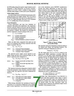
V
CC
47 0.1
6
V
in
V
in
+
-
5.7V
7
5
2
4
R
g
TL494
or
TL594
D
1
1N5819
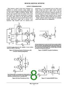
Series gate resistor R may be needed to damp high frequency parasitic oscillations
g
caused by the MOSFET input capacitance and any series wiring inductance in the
gate-source circuit. R will decrease the MOSFET switching speed. Schottky diode
3
g
D can reduce the driver's power dissipation due to excessive ringing, by preventing
The MC34152 greatly enhances the drive capabilities of common switching
regulators and CMOS/TTL logic devices.
1
the output pin from being driven below ground.
Figure 18. Enhanced System Performance with
Common Switching Regulators
Figure 19. MOSFET Parasitic Oscillations
7
4 X
1N5819
5
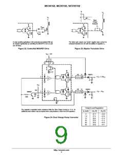
Isolation
Boundary
1N
5819
3
Output Schottky diodes are recommended when driving inductive loads at high
frequencies. The diodes reduce the driver's power dissipation by preventing the
output pins from being driven above V and below ground.
3
CC
Figure 20. Direct Transformer Drive
Figure 21. Isolated MOSFET Drive
http://onsemi.com
8

 ONSEMI [ ONSEMI ]