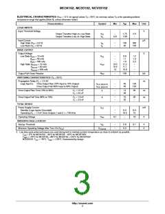
MC34152, MC33152, NCV33152
the NPN pullup during the negative output transient, power
aid in this calculation, power MOSFET manufacturers
provide gate charge information on their data sheets.
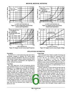
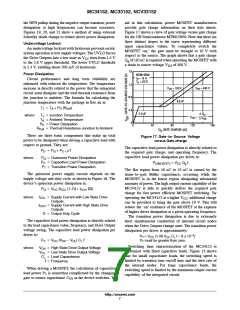
Figure 17 shows a curve of gate voltage versus gate charge
for the ON Semiconductor MTM15N50. Note that there are
three distinct slopes to the curve representing different
input capacitance values. To completely switch the
MOSFET ‘on,’ the gate must be brought to 10 V with
respect to the source. The graph shows that a gate charge
dissipation at high frequencies can become excessive.
Figures 19, 20, and 21 show a method of using external
Schottky diode clamps to reduce driver power dissipation.
Undervoltage Lockout
An undervoltage lockout with hysteresis prevents erratic
system operation at low supply voltages. The UVLO forces
the Drive Outputs into a low state as V rises from 1.4 V
CC
Q of 110 nC is required when operating the MOSFET with
g
to the 5.8 V upper threshold. The lower UVLO threshold
is 5.3 V, yielding about 500 mV of hysteresis.
a drain to source voltage V of 400 V.
DS
16
Power Dissipation
MTM15B50
= 15 A
I
D
Circuit performance and long term reliability are
enhanced with reduced die temperature. Die temperature
increase is directly related to the power that the integrated
circuit must dissipate and the total thermal resistance from
the junction to ambient. The formula for calculating the
junction temperature with the package in free air is:
T = 25°C
A
12
V
DS
ꢁ=ꢁ100ꢁV
V ꢁ=ꢁ400ꢁV
DS
8.0
8.9ꢁnF
TJ = TA + PD (RqJA
)
4.0
0
2.0ꢁnF
DꢁQ
g
where:
TJ = Junction Temperature
TA = Ambient Temperature
PD = Power Dissipation
C
=
GS
DꢁV
GS
0
40
80
Q , GATE CHARGE (nC)
120
160
RqJA = Thermal Resistance Junction to Ambient
g
There are three basic components that make up total
power to be dissipated when driving a capacitive load with
respect to ground. They are:
Figure 17. Gate−to−Source Voltage
versus Gate charge
The capacitive load power dissipation is directly related to
the required gate charge, and operating frequency. The
capacitive load power dissipation per driver is:
PD = PQ + PC + P
T
where:
PQ = Quiescent Power Dissipation
PC = Capacitive Load Power Dissipation
PT = Transition Power Dissipation
PC(MOSFET) = VCC Qg f
The flat region from 10 nC to 55 nC is caused by the
drain−to−gate Miller capacitance, occurring while the
MOSFET is in the linear region dissipating substantial
amounts of power. The high output current capability of the
MC34152 is able to quickly deliver the required gate
charge for fast power efficient MOSFET switching. By
The quiescent power supply current depends on the
supply voltage and duty cycle as shown in Figure 16. The
device’s quiescent power dissipation is:
PQ = VCC (ICCL [1−D] + ICCH [D])
where: ICCL = Supply Current with Low State Drive
operating the MC34152 at a higher V , additional charge
CC
Outputs
can be provided to bring the gate above 10 V. This will
reduce the ‘on’ resistance of the MOSFET at the expense
of higher driver dissipation at a given operating frequency.
The transition power dissipation is due to extremely
short simultaneous conduction of internal circuit nodes
when the Drive Outputs change state. The transition power
dissipation per driver is approximately:
ICCH = Supply Current with High State Drive
Outputs
D = Output Duty Cycle
The capacitive load power dissipation is directly related
to the load capacitance value, frequency, and Drive Output
voltage swing. The capacitive load power dissipation per
driver is:
PT ≈ VCC (1.08 VCC CL f − 8 x 10⁻⁴
PT must be greater than zero.
)
PC = VCC (VOH − VOL) CL f
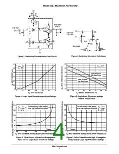
Switching time characterization of the MC34152 is
performed with fixed capacitive loads. Figure 13 shows
that for small capacitance loads, the switching speed is
limited by transistor turn−on/off time and the slew rate of
the internal nodes. For large capacitance loads, the
switching speed is limited by the maximum output current
capability of the integrated circuit.
where: VOH = High State Drive Output Voltage
VOL = Low State Drive Output Voltage
CL = Load Capacitance
f = Frequency
When driving a MOSFET, the calculation of capacitive
load power P is somewhat complicated by the changing
C
gate to source capacitance C as the device switches. To
GS
http://onsemi.com
7

 ONSEMI [ ONSEMI ]