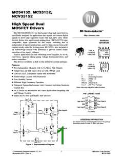
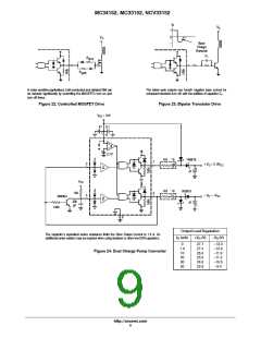
MC34152, MC33152, NCV33152
MAXIMUM RATINGS
Rating
Symbol
Value
20
Unit
V
Power Supply Voltage
Logic Inputs (Note 1)
V
CC
V
in
−0.3 to +V
V
CC
Drive Outputs (Note 2)
A
Totem Pole Sink or Source Current
Diode Clamp Current (Drive Output to V
I
1.5
1.0
O
)
CC
I
O(clamp)
Power Dissipation and Thermal Characteristics
D Suffix, Plastic Package Case 751
Maximum Power Dissipation @ T = 50°C
P
0.56
180
W
°C/W
A
D
Thermal Resistance, Junction−to−Air
R
q
JA
P Suffix, Plastic Package, Case 626
Maximum Power Dissipation @ T = 50°C
P
1.0
100
W
°C/W
A
D
Thermal Resistance, Junction−to−Air
R
q
JA
Operating Junction Temperature
T
+150
°C
°C
J
Operating Ambient Temperature
Operating Ambient Temperature
Operating Ambient Temperature
MC34152
MC33152
MC33152V, NCV33152
T
A
0 to +70
−40 to +85
−40 to +125
Storage Temperature Range
T
stg
−65 to +150
°C
Electrostatic Discharge Sensitivity (ESD)
Human Body Model (HBM)
Machine Model (MM)
ESD
V
2000
200
Stresses exceeding Maximum Ratings may damage the device. Maximum Ratings are stress ratings only. Functional operation above the
RecommendedOperating Conditions is not implied. Extended exposure to stresses above the Recommended Operating Conditions may affect
device reliability.
1. For optimum switching speed, the maximum input voltage should be limited to 10 V or V , whichever is less.
CC
2. Maximum package power dissipation limits must be observed.
http://onsemi.com
2

 ONSEMI [ ONSEMI ]