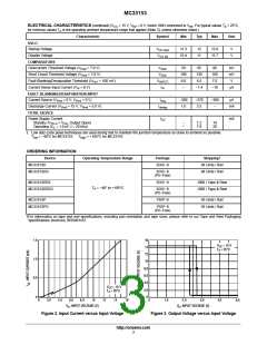
MC33153
MAXIMUM RATINGS
Rating
to V
Symbol
− V
EE
Value
Unit
Power Supply Voltage
V
V
20
V
CC
EE
CC
Kelvin Ground to V (Note 1)
KGND − V
EE
EE
Logic Input
V
V
−0.3 to V
CC
V
V
V
A
in
EE
Current Sense Input
Blanking/Desaturation Input
V
−0.3 to V
S
CC
CC
V
−0.3 to V
BD
Gate Drive Output
Source Current
Sink Current
I
O
1.0
2.0
1.0
Diode Clamp Current
Fault Output
Source Current
Sink Current
I
mA
FO
25
10
Power Dissipation and Thermal Characteristics
D Suffix SO−8 Package, Case 751
Maximum Power Dissipation @ T = 50°C
P
0.56
180
W
°C/W
A
D
JA
Thermal Resistance, Junction−to−Air
P Suffix DIP−8 Package, Case 626
R
q
Maximum Power Dissipation @ T = 50°C
1.0
100
W
°C/W
A
D
JA
Thermal Resistance, Junction−to−Air
Operating Junction Temperature
T
+150
°C
°C
°C
J
Operating Ambient Temperature
T
A
−40 to +105
−65 to +150
Storage Temperature Range
T
stg
NOTE: ESD data available upon request.
Stresses exceeding Maximum Ratings may damage the device. Maximum Ratings are stress ratings only. Functional operation above the
Recommended Operating Conditions is not implied. Extended exposure to stresses above the Recommended Operating Conditions may affect
device reliability.
1. Kelvin Ground must always be between V and V
.
EE
CC
ELECTRICAL CHARACTERISTICS (V = 15 V, V = 0 V, Kelvin GND connected to V . For typical values T = 25°C,
CC
EE
EE
A
for min/max values T is the operating ambient temperature range that applies (Note 2), unless otherwise noted.)
A
Characteristic
Symbol
Min
Typ
Max
Unit
LOGIC INPUT
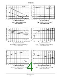
Input Threshold Voltage
High State (Logic 1)
Low State (Logic 0)
V
V
V
−
1.2
2.70
2.30
3.2
−
IH
IL
Input Current
mA
High State (V = 3.0 V)
Low State (V = 1.2 V)
I
I
−
−
130
50
500
100
IH
IL
IH
IL
DRIVE OUTPUT
Output Voltage
V
Low State (I
High State (I
= 1.0 A)
V
−
12
2.0
13.9
2.5
−
Sink
OL
= 500 mA)
V
Source
OH
Output Pull−Down Resistor
R
PD
−
100
200
kW
FAULT OUTPUT
Output Voltage
V
Low State (I
High State (I
= 5.0 mA)
V
−
12
0.2
13.3
1.0
−
Sink
FL
= 20 mA)
V
Source
FH
SWITCHING CHARACTERISTICS
Propagation Delay (50% Input to 50% Output C = 1.0 nF)
ns
L
Logic Input to Drive Output Rise
Logic Input to Drive Output Fall
t
−
−
80
120
300
300
PLH(in/out)
t
PHL (in/out)
Drive Output Rise Time (10% to 90%) C = 1.0 nF
t
t
−
−
−
17
17
55
55
ns
ns
ms
L
r
Drive Output Fall Time (90% to 10%) C = 1.0 nF
L
f
Propagation Delay
Current Sense Input to Drive Output
Fault Blanking/Desaturation Input to Drive Output
t
t
0.3
1.0
P(OC)
P(FLT)
2. Low duty cycle pulse techniques are used during test to maintain the junction temperature as close to ambient as possible.
= −40°C for MC33153 = +105°C for MC33153
T
T
high
low
http://onsemi.com
2

 ONSEMI [ ONSEMI ]