MC100LVE210
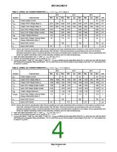
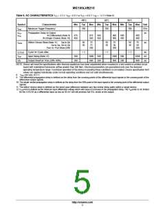
Z = 50 W
Q
Q
D
D
o
Receiver
Device
Driver
Device
Z = 50 W
o
50 W
50 W
V
TT
V
= V − 2.0 V
TT
CC
Figure 3. Typical Termination for Output Driver and Device Evaluation
(See Application Note AND8020/D − Termination of ECL Logic Devices.)
ORDERING INFORMATION
†
Device
MC100LVE210FN
Package
Shipping
PLCC−28
37 Units / Rail
37 Units / Rail
MC100LVE210FNG
PLCC−28
(Pb−Free)
MC100LVE210FNR2
MC100LVE210FNR2G
PLCC−28
500 Tape & Reel
500 Tape & Reel
PLCC−28
(Pb−Free)
†For information on tape and reel specifications, including part orientation and tape sizes, please refer to our Tape and Reel Packaging
Specifications Brochure, BRD8011/D.
Resource Reference of Application Notes
AN1405/D
AN1406/D
AN1503/D
AN1504/D
AN1568/D
AN1672/D
AND8001/D
AND8002/D
AND8020/D
AND8066/D
AND8090/D
−
−
−
−
−
−
−
−
−
−
−
ECL Clock Distribution Techniques
Designing with PECL (ECL at +5.0 V)
ECLinPSt I/O SPiCE Modeling Kit
Metastability and the ECLinPS Family
Interfacing Between LVDS and ECL
The ECL Translator Guide
Odd Number Counters Design
Marking and Date Codes
Termination of ECL Logic Devices
Interfacing with ECLinPS
AC Characteristics of ECL Devices
http://onsemi.com
6

 ONSEMI [ ONSEMI ]