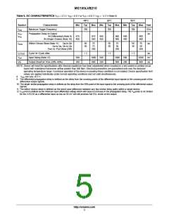
MC100LVE210
3.3VꢀECL Dual 1:4, 1:5
Differential Fanout Buffer
Description
The MC100LVE210 is a low voltage, low skew dual differential ECL
fanout buffer designed with clock distribution in mind. The device features
two fanout buffers, a 1:4 and a 1:5 buffer, on a single chip. The device
features fully differential clock paths to minimize both device and system
skew. The dual buffer allows for the fanout of two signals through a single
chip, thus reducing the skew between the two fundamental signals from a
part−to−part skew down to an output−to−output skew. This capability
reduces the skew by a factor of 4 as compared to using two LVE111’s to
accomplish the same task.
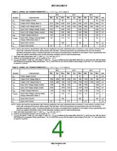
To ensure that the tight skew specification is met it is necessary that both
sides of the differential output are identically terminated, even if only one
side is being used. In most applications all nine differential pairs will be
used and therefore terminated. In the case where fewer than nine pairs are
used it is necessary to terminate at least the output pairs adjacent to the
output pair being used in order to maintain minimum skew. Failure to
follow this guideline will result in small degradations of propagation delay
(on the order of 10−20 ps) of the outputs being used, while not catastrophic
to most designs this will result in an increase in skew. Note that the
package corners isolate outputs from one another such that the guideline
expressed above holds only for outputs on the same side of the package.
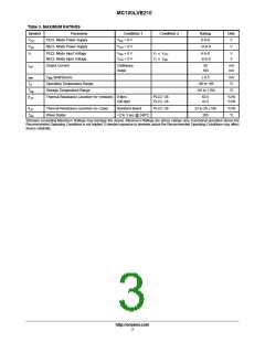
The MC100LVE210, as with most ECL devices, can be operated from a
http://onsemi.com
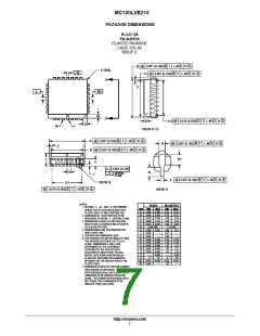
MARKING
DIAGRAM*
128
MC100LVE210G
AWLYYWW
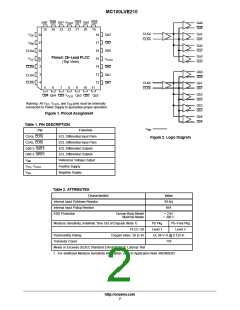
PLCC−28
FN SUFFIX
CASE 776
A
= Assembly Location
WL
YY
WW
G
= Wafer Lot
= Year
= Work Week
= Pb−Free Package
positive V supply in PECL mode. This allows the LVE210 to be used
CC
*For additional marking information, refer to
Application Note AND8002/D.
for high performance clock distribution in +3.3 V systems. Designers can
take advantage of the LVE210’s performance to distribute low skew clocks
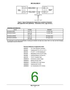
across the backplane or the board. In a PECL environment series or
Thevenin line terminations are typically used as they require no additional
power supplies, if parallel termination is desired a terminating voltage of
ORDERING INFORMATION
See detailed ordering and shipping information in the package
dimensions section on page 6 of this data sheet.
V
CC
− 2.0 V will need to be provided. For more information on using
PECL, designers should refer to Application Note AN1406/D.
The V pin, an internally generated voltage supply, is available to this
BB
device only. For single-ended input conditions, the unused differential
input is connected to V as a switching reference voltage. V may also
BB
BB
rebias AC coupled inputs. When used, decouple V and V via a
BB
CC
0.01 mF capacitor and limit current sourcing or sinking to 0.5 mA. When
not used, V should be left open.
BB
Features
• 200 ps Part−to−Part Skew
• 50 ps Typical Output−to−Output Skew
• The 100 Series Contains Temperature Compensation
• PECL Mode Operating Range: V = 3.0 V to 3.8 V with V = 0 V
CC
EE
• NECL Mode Operating Range: V = 0 V with V = −3.0 V to −3.8 V
CC
EE
• Internal Input Pulldown Resistors
• Q Output will Default LOW with Inputs Open or at V
• Pb−Free Packages are Available*
EE
*For additional information on our Pb−Free strategy and soldering details, please
download the ON Semiconductor Soldering and Mounting Techniques
Reference Manual, SOLDERRM/D.
©
Semiconductor Components Industries, LLC, 2006
1
Publication Order Number:
December, 2006 − Rev. 7
MC100LVE210/D

 ONSEMI [ ONSEMI ]