MC100LVE210
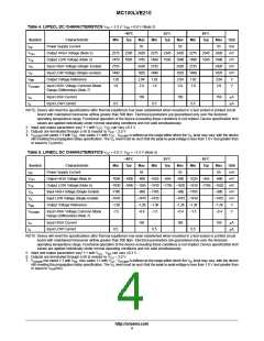
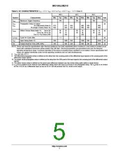
Table 4. LVPECL DC CHARACTERISTICS V = 3.3 V; V = 0.0 V (Note 2)
CC
EE
−40°C
25°C
85°C
Symbol
Characteristic
Power Supply Current
Min
Typ
Max
55
Min
Typ
Max
55
Min
Typ
Max
65
Unit
mA
mV
mV
mV
mV
V
I
EE
V
Output HIGH Voltage (Note 3)
Output LOW Voltage (Note 3)
Input HIGH Voltage (Single−Ended)
Input LOW Voltage (Single−Ended)
Output Voltage Reference
2215
1470
2135
1490
1.92
1.8
2295
1605
2420
1745
2420
1825
2.04
2.9
2275
1490
2135
1490
1.92
1.8
2345
1595
2420
1680
2420
1825
2.04
2.9
2275
1490
2135
1490
1.92
1.8
2345
1595
2420
1680
2420
1825
2.04
2.9
OH
OL
V
V
V
V
V
IH
IL
BB
Input HIGH Voltage Common Mode
Range (Differential) (Note 7)
V
IHCMR
I
I
Input HIGH Current
Input LOW Current
150
150
150
mA
mA
IH
IL
0.5
0.5
0.5
NOTE: Device will meet the specifications after thermal equilibrium has been established when mounted in a test socket or printed circuit
board with maintained transverse airflow greater than 500 lfpm. Electrical parameters are guaranteed only over the declared
operating temperature range. Functional operation of the device exceeding these conditions is not implied. Device specification limit
values are applied individually under normal operating conditions and not valid simultaneously.
2. Input and output parameters vary 1:1 with V . V can vary 0.3 V.
CC
EE
3. Outputs are terminated through a 50 W resistor to V − 2.0 V.
CC
4. V
min varies 1:1 with V , max varies 1:1 with V . V
is defined as the range within which the V level may vary, with the device
IHCMR
EE
CC
IHCMR IH
still meeting the propagation delay specification. The V level must be such that the peak to peak voltage is less than 1.0 V and greater than
IL
or equal to V (min).
PP
Table 5. LVNECL DC CHARACTERISTICS V = 0.0 V; V = −3.3 V (Note 5)
CC
EE
−40°C
25°C
85°C
Symbol
Characteristic
Power Supply Current
Min
Typ
Max
Min
Typ
Max
Min
Typ
Max
65
Unit
mA
mV
mV
mV
mV
V
I
55
55
EE
V
Output HIGH Voltage (Note 6)
Output LOW Voltage (Note 6)
Input HIGH Voltage (Single−Ended)
Input LOW Voltage (Single−Ended)
Output Voltage Reference
−1085 −1005 −880 −1025 −955
−880 −1025 −955
−880
OH
OL
V
V
V
V
V
−1830 −1695 −1555 −1810 −1705 −1620 −1810 −1705 −1620
−1165
−1810
−1.38
−1.5
−880 −1165
−1475 −1810
−1.26 −1.38
−880 −1165
−1475 −1810
−1.26 −1.38
−880
−1475
−1.26
−0.4
IH
IL
BB
Input HIGH Voltage Common Mode
Range (Differential) (Note 7)
−0.4
−1.5
−0.4
−1.5
V
IHCMR
I
I
Input HIGH Current
Input LOW Current
150
150
150
mA
mA
IH
IL
0.5
0.5
0.5
NOTE: Device will meet the specifications after thermal equilibrium has been established when mounted in a test socket or printed circuit
board with maintained transverse airflow greater than 500 lfpm. Electrical parameters are guaranteed only over the declared
operating temperature range. Functional operation of the device exceeding these conditions is not implied. Device specification limit
values are applied individually under normal operating conditions and not valid simultaneously.
5. Input and output parameters vary 1:1 with V . V can vary 0.3 V.
CC
EE
6. Outputs are terminated through a 50 W resistor to V − 2.0 V.
CC
7. V
min varies 1:1 with V , max varies 1:1 with V . V
is defined as the range within which the V level may vary, with the device
IHCMR
EE
CC
IHCMR IH
still meeting the propagation delay specification. The V level must be such that the peak to peak voltage is less than 1.0 V and greater than
IL
or equal to V (min).
PP
http://onsemi.com
4

 ONSEMI [ ONSEMI ]