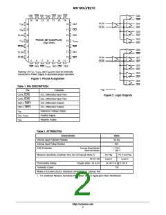
MC100LVE210
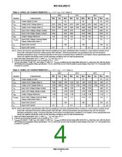
Table 3. MAXIMUM RATINGS
Symbol
Parameter
Condition 1
Condition 2
Rating
8 to 0
Unit
V
V
V
V
PECL Mode Power Supply
NECL Mode Power Supply
V
V
= 0 V
= 0 V
CC
EE
I
EE
CC
−8 to 0
V
PECL Mode Input Voltage
NECL Mode Input Voltage
V
V
= 0 V
= 0 V
V v V
6 to 0
V
V
EE
CC
I
CC
EE
V w V
−6 to 0
I
I
I
Output Current
Continuous
Surge
50
100
mA
mA
out
V
Sink/Source
BB
0.5
mA
°C
BB
T
A
Operating Temperature Range
Storage Temperature Range
−40 to +85
−65 to +150
T
stg
°C
q
Thermal Resistance (Junction−to−Ambient) 0 lfpm
500 lfpm
PLCC−28
PLCC−28
63.5
43.5
°C/W
°C/W
JA
q
Thermal Resistance (Junction−to−Case)
Wave Solder
Standard Board
PLCC−28
22 to 26 5%
265
°C/W
°C
JC
T
sol
<2 to 3 sec @ 248°C
Stresses exceeding Maximum Ratings may damage the device. Maximum Ratings are stress ratings only. Functional operation above the
Recommended Operating Conditions is not implied. Extended exposure to stresses above the Recommended Operating Conditions may affect
device reliability.
http://onsemi.com
3

 ONSEMI [ ONSEMI ]