MC100LVE210
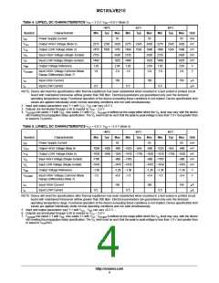
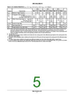
Table 6. AC CHARACTERISTICS V = 3.3 V; V = 0.0 V or V = 0.0 V; V = −3.3 V (Note 8)
CC
EE
CC
−40°C
Typ
EE
25°C
Typ
700
85°C
Typ
700
Symbol
Characteristic
Min
Max
Min
Max
Min
Max
Unit
GHz
ps
f
Maximum Toggle Frequency
Propagation Delay to Output
700
max
t
t
PLH
PHL
IN (Differential) (Note 9)
IN (Single−Ended) (Note 10)
475
400
875
850
500
450
900
900
500
450
900
900
t
t
Within−Device Skew (Note 11)
Qa to Qb
50
50
75
75
200
50
30
75
50
200
50
30
75
50
200
ps
skew
Qa to Qa, Qb to Qb
Part−to−Part Skew (Diff)
Cycle−to−Cycle Jitter
< 1
< 1
< 1
ps
mV
ps
JITTER
V
Input Swing (Note 12)
500
200
1000
600
500
200
1000
600
500
200
1000
600
PP
t /t
Output Rise/Fall Time (20%−80%)
r
f
NOTE: Device will meet the specifications after thermal equilibrium has been established when mounted in a test socket or printed circuit
board with maintained transverse airflow greater than 500 lfpm. Electrical parameters are guaranteed only over the declared
operating temperature range. Functional operation of the device exceeding these conditions is not implied. Device specification limit
values are applied individually under normal operating conditions and not valid simultaneously.
8.
V
can vary 0.3 V.
EE
9. The differential propagation delay is defined as the delay from the crossing points of the differential input signals to the crossing point of the
differential output signals.
10.The single−ended propagation delay is defined as the delay from the 50% point of the input signal to the crossing point of the differential output
signals.
11. The within−device skew is defined as the worst case difference between any two similar delay paths within a single device.
12.V (min) is defined as the minimum input differential voltage which will cause no increase in the propagation delay. The V (min) is AC limited
PP
PP
for the LVE210 as a differential input as low as 50 mV will still produce full ECL levels at the output.
http://onsemi.com
5

 ONSEMI [ ONSEMI ]