DC Electrical Characteristics
All typical values are at 25ºC unless otherwise specified.
TA = -40 to +85°C
Symbol
Parameter
VCC (V)
Conditions
Unit
Min. Typ.(5) Max.
Common Pins
VIK
Clamp Diode Voltage
3.0
IIK = -18mA
-1.2
Control Input Voltage
HIGH
VIH
2.7 to 4.3
1.7
V
Control Input Voltage
LOW
VIL
IIN
2.7 to 4.3
4.3
0.6
/OE Input Leakage
Current
µA
µA
VIN = 4.3V
1
-1
Power Off Leakage
Current (Common Port
Only /R, /L)
Common Port (/R, /L)
IOFF
0
-10
10
VSW = 4.3V or Floating
/R, /L = 0.3V, 4.0V
R, L = Floating
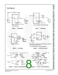
Figure 8
On-Leakage Current of
Port /R or /L
INC(0N)
4.3
-250
1
250
nA
/OE Internal Pull-Up
Resistor
RPu,
RT
4.3
4.3
3
MΩ
Ω
Audio Path Termination
Resistors
VIN=0.3V or 4.0V
100
VCC-
4.3V
VAudio
Analog Signal Range
2.7 to 4.3
VCC
3.0
V
VL/R = -1.5V, 0V,1.5V
RONAudio
Switch On Resistance(2)
2.7
1.5
Ω
I
ON = 60ma
(3)
∆RONAudio Delta RON
RFLAT(Audio) RON Flatness(4)
Power Supply
2.7
2.7
VL/R = 0.7V ION = 60mA
VSW=-1.5V to 1.5V,
0.4
0.4
Ω
Ω
0.8
15
I
ON = 60mA
ICC
Quiescent Supply Current
4.3
/OE = Low or VCC, IOUT = 0
1.5
µA
Notes:
2. On resistance is determined by the voltage drop between the A and B pins at the indicated current through the switch.
3. ∆ RON = RON max – RON min measured at identical VCC, temperature, and voltage.
4. Flatness is defined as the difference between the maximum and minimum values of on resistance over the
specified range of conditions.
5. Guaranteed by characterization; not production tested.
© 2008 Fairchild Semiconductor Corporation
FSA2147 Rev. 1.0.1
www.fairchildsemi.com
4

 ONSEMI [ ONSEMI ]