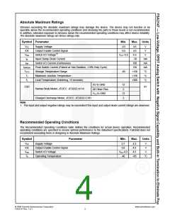
Absolute Maximum Ratings
Stresses exceeding the absolute maximum ratings may damage the device. The device may not function or be
operable above the recommended operating conditions and stressing the parts to these levels is not recommended.
In addition, extended exposure to stresses above the recommended operating conditions may affect device reliability.
The absolute maximum ratings are stress ratings only.
Symbol Parameter
Min.
Max. Units
VCC
/OE
VSW
IIK
Supply Voltage
-0.5
-0.5
4.6
4.6
V
V
Output Enable Control Signal
Switch I/O Voltage(1)
VCC–4.6
4.6
V
Input Clamp Diode Current
- 50
100
150
+150
+150
+260
mA
mA
mA
°C
°C
°C
ISW
Switch I/O Current (Continuous)
Peak Switch Current (Pulsed at 1ms Duration, <10% Duty Cycle)
Storage Temperature Range
ISWPEAK
TSTG
TJ
-65
12
Maximum Junction Temperature
Lead Temperature (Soldering, 10 seconds)
TL
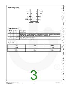
I/O to GND
ESD
kV
Human Body Model, JEDEC: JESD22-A114
All Other Pins
VCC to GND
2
12
Charged Discharge Model, JEDEC: JESD22-C101
2
Note:
1. The input and output negative ratings may be exceeded if the input and output diode current ratings are observed.
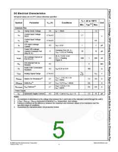
Recommended Operating Conditions
The Recommended Operating Conditions table defines the conditions for actual device operation. Recommended
operating conditions are specified to ensure optimal performance to the datasheet specifications. Fairchild does not
recommend exceeding them or designing to Absolute Maximum Ratings.
Symbol
Parameter
Min.
Max.
Units
VCC
/OE
VSW
TA
Supply Voltage
2.7
3.0
4.3
4.3
4.3
+85
V
V
Output Enable Control Signal
Switch I/O Voltage
VCC -4.3
-40
V
Operating Temperature
°C
© 2008 Fairchild Semiconductor Corporation
FSA2147 Rev. 1.0.1
www.fairchildsemi.com
3

 ONSEMI [ ONSEMI ]