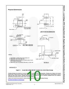
Physical Dimensions
1.80
0.15
8
5
0.70
-B-
2.3±0.1
3.1±.1
1.00
1.55
0.30 TYP
1
4
0.2 C B A
ALL LEAD TIPS
0.5 TYP
PIN #1 IDENT.
ALL LEAD TIPS
0.1 C
DETAIL A
0.70±0.10
0.90 MAX
-C-
0.10-0.18
0.10
0.00
0.17-0.27
0.13
A B
C
0.50TYP
0.4 TYP
GAGE PLANE
0.12
0°-8°
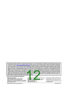
A. CONFORMS TO JEDEC REGISTRATION MO-187
B. DIMENSIONS ARE IN MILLIMETERS.
SEATING PLANE
C. DIMENSIONS ARE EXCLUSIVE OF BURRS, MOLD FLASH,
AND TIE BAR EXTRUSIONS.
D. DIMENSIONS AND TOLERANCES PER ANSI Y14.5M, 1982.
DETAIL A
MAB08AREVC
Figure 17. 8-Lead US8, JEDEC MO-187, Variation CA, 3.0mm Wide Package
Package drawings are provided as a service to customers considering Fairchild components. Drawings may change in any manner
without notice. Please note the revision and/or date on the drawing and contact a Fairchild Semiconductor representative to verify or
obtain the most recent revision. Package specifications do not expand the terms of Fairchild’s worldwide terms and conditions,
specifically the warranty therein, which covers Fairchild products.
Always visit Fairchild Semiconductor’s online packaging area for the most recent package drawings:
http://www.fairchildsemi.com/packaging/.
© 2008 Fairchild Semiconductor Corporation
FSA2147 Rev. 1.0.1
www.fairchildsemi.com
9

 ONSEMI [ ONSEMI ]