March 2015
FDD86102
N-Channel Shielded Gate PowerTrench® MOSFET
100 V, 36 A, 24 mΩ
Features
General Description
This N-Channel MOSFET is produced using Fairchild
Semiconductor‘s advanced PowerTrench® process that
incorporates Shielded Gate technology. This process has been
optimized for rDS(on), switching performance and ruggedness.
Shielded Gate MOSFET Technology
Max rDS(on) = 24 mΩ at VGS = 10 V, ID = 8 A
Max rDS(on) = 38 mΩ at VGS = 6 V, ID = 6 A
High performance trench technology for extremely low rDS(on)
High power and current handling capability in a widely used
surface mount package
Application
DC - DC Conversion
Very low Qg and Qgd compared to competing trench
technologies
Fast switching speed
100% UIL tested
RoHS Compliant
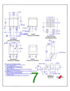
D
D
G
G
S
D-PAK
TO -252
(TO-252)
S
MOSFET Maximum Ratings TC = 25 °C unless otherwise noted
Symbol
VDS
VGS
Parameter
Ratings
Units
Drain to Source Voltage
Gate to Source Voltage
Drain Current -Continuous
-Continuous
100
V
V
±20
TC = 25 °C
TA = 25 °C
36
ID
(Note 1a)
(Note 4)
(Note 3)
8
75
A
-Pulsed
EAS
Single Pulse Avalanche Energy
Power Dissipation
121
mJ
W
TC = 25 °C
TA = 25 °C
62
PD
Power Dissipation
(Note 1a)
3.1
TJ, TSTG
Operating and Storage Junction Temperature Range
-55 to +150
°C
Thermal Characteristics
RθJC
RθJA
Thermal Resistance, Junction to Case
Thermal Resistance, Junction to Ambient
2.0
40
°C/W
(Note 1a)
Package Marking and Ordering Information
Device Marking
Device
Package
Reel Size
13 ’’
Tape Width
16 mm
Quantity
FDD86102
FDD86102
D-PAK(TO-252)
2500 units
1
©2012 Fairchild Semiconductor Corporation
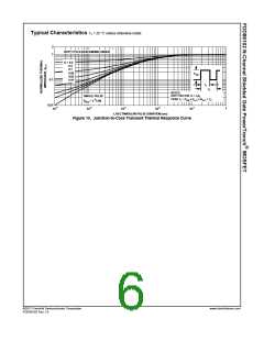
FDD86102 Rev.1.9
www.fairchildsemi.com

 ONSEMI [ ONSEMI ]