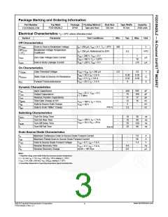
Typical Performance Characteristics
Figure 1. On-Region Characteristics
Figure 2. Transfer Characteristics
20
30
VGS = 10V
7V
10
5V
4.5V
4V
10
3.5V
150oC
25oC
1
1
-55oC
*Notes:
1. 250μs Pulse Test
2. TC = 25oC
* Notes :
1. VDS = 20V
2. 250μs Pulse Test
0.1
0.1
0.1
1
10
2
3
4
5
6
VDS, Drain-Source Voltage[V]
VGS, Gate-Source Voltage[V]
Figure 3. On-Resistance Variation vs.
Drain Current and Gate Voltage
Figure 4. Body Diode Forward Voltage
Variation vs. Source Current
and Temperature
1.0
50
0.8
VGS = 10V
10
150oC
0.6
25oC
VGS = 20V
0.4
Notes:
1. VGS = 0V
* Note : TJ = 25oC
15 20 25
2. 250μs Pulse Test
0.2
1
0
5
10
ID, Drain Current [A]
0.4
0.8
1.2
1.6
VSD, Body Diode Forward Voltage [V]
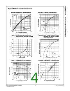
Figure 5. Capacitance Characteristics
Figure 6. Gate Charge Characteristics
10
1000
Ciss
8
VDS = 50V
VDS = 100V
100
V
DS = 160V
Coss
6
4
2
0
* Note:
1. VGS = 0V
Crss
10
2. f = 1MHz
C
C
C
= C + C (C = shorted)
gs gd ds
iss
= C + C
ds gd
oss
rss
* Note : ID = 7.6A
9
= C
gd
1
0
3
6
12
0.1
1
10
30
Qg, Total Gate Charge [nC]
VDS, Drain-Source Voltage [V]
www.fairchildsemi.com
©2010 Fairchild Semiconductor Corporation
FDD10N20LZ Rev. C1
3

 ONSEMI [ ONSEMI ]