Package Marking and Ordering Information
Part Number
Top Mark
Package
Packing Method
Reel Size
Tape Width
Quantity
FDD10N20LZ
DPAK
Tape and Reel
330 mm
16 mm
2500 units
FDD10N20LZTM
Electrical Characteristics TC = 25oC unless otherwise noted.
Symbol
Parameter
Test Conditions
Min.
Typ.
Max.
Unit
Off Characteristics
BVDSS
Drain to Source Breakdown Voltage
ID = 250 μA, VGS = 0 V, TC = 25oC
D = 250 μA, Referenced to 25oC
DS = 200 V, VGS = 0 V
200
-
-
-
-
V
ΔBVDSS
/ ΔTJ
Breakdown Voltage Temperature
Coefficient
I
0.2
V/oC
V
-
-
-
-
-
-
1
IDSS
IGSS
Zero Gate Voltage Drain Current
Gate to Body Leakage Current
μA
μA
VDS = 160 V, TC = 125oC
10
VGS = ±20 V, VDS = 0 V
±10
On Characteristics
VGS(th)
RDS(on)
gFS
Gate Threshold Voltage
VGS = VDS, ID = 250 μA
2.0
-
3.0
0.36
0.38
-
V
Ω
S
V
GS = 10 V, ID = 3.8 A
-
-
-
0.30
0.32
8
Static Drain to Source On Resistance
Forward Transconductance
VGS = 5 V, ID = 3.8 A
VDS = 20 V, ID = 3.8 A
Dynamic Characteristics
Ciss
Input Capacitance
-
-
-
-
-
-
440
75
11
585
100
17
16
-
pF
pF
pF
nC
nC
nC
VDS = 25 V, VGS = 0 V,
f = 1 MHz
Coss
Crss
Qg(tot)
Qgs
Output Capacitance
Reverse Transfer Capacitance
Total Gate Charge at 10V
Gate to Source Gate Charge
Gate to Drain “Miller” Charge
12
2
V
V
DS = 100 V, ID = 7.6 A,
GS = 10 V
(Note 4)
Qgd
3.5
-
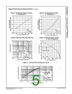
Switching Characteristics
td(on)
tr
td(off)
tf
Turn-On Delay Time
Turn-On Rise Time
Turn-Off Delay Time
Turn-Off Fall Time
-
-
-
-
10
15
55
25
30
40
ns
ns
ns
ns
VDD = 100 V, ID = 7.6 A,
GS = 10 V, RG = 25 Ω
V
120
60
(Note 4)
Drain-Source Diode Characteristics
IS
Maximum Continuous Drain to Source Diode Forward Current
Maximum Pulsed Drain to Source Diode Forward Current
-
-
-
-
-
-
-
7.6
30
1.4
-
A
A
ISM
VSD
trr
Drain to Source Diode Forward Voltage
Reverse Recovery Time
VGS = 0 V, ISD = 7.6 A
-
V
115
0.5
ns
μC
VGS = 0 V, ISD = 7.6 A,
dIF/dt = 100 A/μs
Qrr
Reverse Recovery Charge
-
Notes:
1. Repetitive rating: pulse-width limited by maximum junction temperature.
2. L = 4.2 mH, I = 7.6 A, V = 50 V, R = 25 Ω, starting T = 25°C.
AS
DD
G
J
3. I ≤ 7.6 A, di/dt ≤ 200 A/μs, V ≤ BV
, starting T = 25°C.
SD
DD
DSS
J
4. Essentially independent of operating temperature typical characteristics.
www.fairchildsemi.com
©2010 Fairchild Semiconductor Corporation
FDD10N20LZ Rev. C1
2

 ONSEMI [ ONSEMI ]