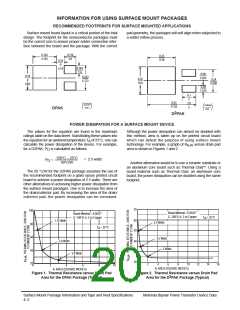
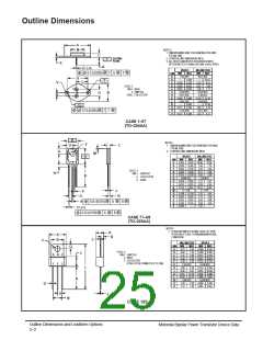
Prior to placing surface mount components onto a printed
circuit board, solder paste must be applied to the pads.
Solder stencils are used to screen the optimum amount.
These stencils are typically 0.008 inches thick and may be
made of brass or stainless steel. This is not the case with the
SOLDER PASTE
OPENINGS
2
DPAK and D PAK packages. If a 1:1 opening is used to
screen solder onto the drain pad, misalignment and/or “tomb-
stoning” may occur due to an excess of solder. For these two
packages, the opening in the stencil for the paste should be
approximately 50% of the tab area. The opening for the leads
is still a 1:1 registration. Figure 3 shows a typical stencil for
STENCIL
Figure 3. Typical Stencil for DPAK and
2
the DPAK and D PAK packages. The pattern of the opening
2
D PAK Packages
in the stencil for the drain pad is not critical as long as it
allows approximately 50% of the pad to be covered with
paste.
SOLDERING PRECAUTIONS
The melting temperature of solder is higher than the rated
temperature of the device. When the entire device is heated
to a high temperature, failure to complete soldering within a
short time could result in device failure. Therefore, the
following items should always be observed in order to mini-
mize the thermal stress to which the devices are subjected.
• Always preheat the device.
• After soldering has been completed, the device should be
allowed to cool naturally for at least three minutes.
Gradual cooling should be used since the use of forced
cooling will increase the temperature gradient and will
result in latent failure due to mechanical stress.
• Mechanical stress or shock should not be applied during
cooling.
• The delta temperature between the preheat and soldering
should be 100°C or less.*
* Soldering a device without preheating can cause excessive
thermal shock and stress which can result in damage to the
device.
• When preheating and soldering, the temperature of the
leads and the case must not exceed the maximum
temperature ratings as shown on the data sheet. When
using infrared heating with the reflow soldering method,
the difference should be a maximum of 10°C.
* Due to shadowing and the inability to set the wave height to
2
incorporate other surface mount components, the D PAK is
• The soldering temperature and time should not exceed
260°C for more than 10 seconds.
not recommended for wave soldering.
• When shifting from preheating to soldering, the maximum
temperature gradient shall be 5°C or less.
Surface Mount Package Information and Tape and Reel Specifications
4–3
Motorola Bipolar Power Transistor Device Data

 ONSEMI [ ONSEMI ]