Audio
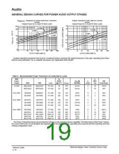
GENERAL DESIGN CURVES FOR POWER AUDIO OUTPUT STAGES
V
Required on Output and Driver Transistor
versus
Output Transistor Peak Collector Current
versus
(BR)CEO
Output Power for 4, 8 and 18 Ohm Loads
Output Power for 4, 8 and 16 Ohm Loads
50
30
500
16 OHMS
8 OHMS
300
4 OHMS
8 OHMS
4 OHMS
10
100
70
50
16 OHMS
5.0
3.0
30
1.0
10
10
10
30
50
100
300
500
1000
30
50
100
300
500
1000
OUTPUT POWER (WATTS)
OUTPUT POWER (WATTS)
Another important parameter that must be considered before selecting the output transistors is the safe–operating area these
devices must withstand. For a complete discussion see Application Note AN485.
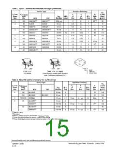
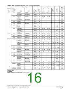
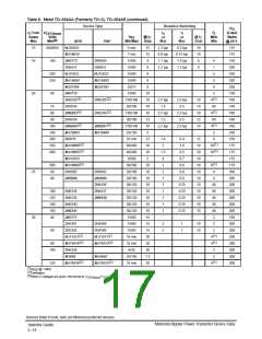
Table 9. Recommended Power Transistors for Audio/Servo Loads
RMS
Power
Output
P
f
T
MHz
Typ
D
Watts
@ 25°C
h
@
I
ISB
Volts/Amps
FE
C
NPN
PNP
Case
V
CEO
Min/Max
Amps
To 25W
25 to 50W
50 to 100W
MJE15030
MJE15032
MJE15031
MJE15033
TO–220
TO–220
50
50
150
250
20 min
50 min
4
1
30
40
14/3.6
50/1
2N3055A
MJ15001
MJ2955A
MJ15002
TO–204
TO–204
120
200
120
140
20/70
4
4
3
3
60/2
40/5
25/150
MJ15015
MJ15003
MJ15020
MJ15016
MJ15004
MJ15021
TO–204
TO–204
TO–204
180
250
150
120
140
250
20/70
25/150
30 min
4
5
1
3
3
60/3
100/1
50/3
20
Over 100W
MJ15024
MJ15025
TO–204
250
250
15/60
8
8
80/2.2
MJ3281A
MJL3281A
MJ21194
MJ1302A
MJL1302A
MJ21193
TO–204
340G–01
TO–204
340G–01
250
150
250
200
200
200
250
200
60/175
60/175
25/75
7
7
8
8
30
30
7
50/4
40/4
100/2
100/2
MJL21194
MJL21193
25/75
7
The Power Transistors shown are provided for reference only and show device capability. The final choice of the Power Transis-
tors used is left to the circuit designer and depends upon the particular safe–operating area required and the mounting and heat
sinking configuration used.
Motorola Bipolar Power Transistor Device Data
Selector Guide
2–16

 ONSEMI [ ONSEMI ]