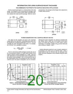
INFORMATION FOR USING SURFACE MOUNT PACKAGES
RECOMMENDED FOOTPRINTS FOR SURFACE MOUNTED APPLICATIONS
Surface mount board layout is a critical portion of the total
pad geometry, the packages will self align when subjected to
design. The footprint for the semiconductor packages must
be the correct size to ensure proper solder connection inter-
face between the board and the package. With the correct
a solder reflow process.
0.165
4.191
0.118
3.0
0.33
8.38
0.10
0
0.063
1.6
2.54
0.08
2.032
0.19
0
4.82
6
0.243
6.172
0.42
10.6
6
0.24
6.096
0.04
1.016
0.1
2
0.63
17.02
3.0
5
inches
mm
inches
mm
DPAK
2
D PAK
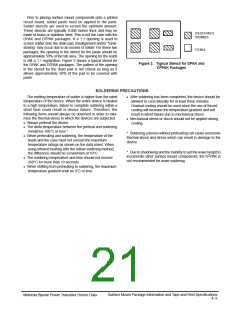
POWER DISSIPATION FOR A SURFACE MOUNT DEVICE
The values for the equation are found in the maximum
ratings table on the data sheet. Substituting these values into
Although the power dissipation can almost be doubled with
this method, area is taken up on the printed circuit board
which can defeat the purpose of using surface mount
the equation for an ambient temperature T of 25°C, one can
A
calculate the power dissipation of the device. For example,
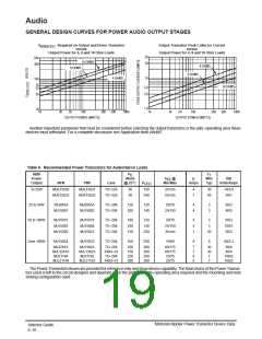
technology. For example, a graph of R
area is shown in Figures 1 and 2.
versus drain pad
θJA
for a D2PAK, P is calculated as follows.
D
150°C – 25°C
= 2.5 watts
P
=
D
50°C/W
Another alternative would be to use a ceramic substrate or
an aluminum core board such as Thermal Clad . Using a
board material such as Thermal Clad, an aluminum core
board, the power dissipation can be doubled using the same
footprint.
The 50 °C/W for the D2PAK package assumes the use of
the recommended footprint on a glass epoxy printed circuit
board to achieve a power dissipation of 2.5 watts. There are
other alternatives to achieving higher power dissipation from
the surface mount packages. One is to increase the area of
the drain/collector pad. By increasing the area of the drain/
collector pad, the power dissipation can be increased.
70
100
Board Material = 0.0625″
G–10/FR–4, 2 oz Copper
Board Material = 0.0625″
G–10/FR–4, 2 oz Copper
T = 25°C
A
60
50
1.75 Watts
80
2.5 Watts
3.5 Watts
T = 25°C
A
60
40
20
3.0 Watts
40
30
20
5 Watts
5.0 Watts
2
0
4
6
8
10
12
14
16
0
2
4
6
8
10
A, AREA (SQUARE INCHES)
A, AREA (SQUARE INCHES)
Figure 1. Thermal Resistance versus Drain Pad
Area for the DPAK Package (Typical)
Figure 2. Thermal Resistance versus Drain Pad
2
Area for the D PAK Package (Typical)
Surface Mount Package Information and Tape and Reel Specifications
4–2
Motorola Bipolar Power Transistor Device Data

 ONSEMI [ ONSEMI ]