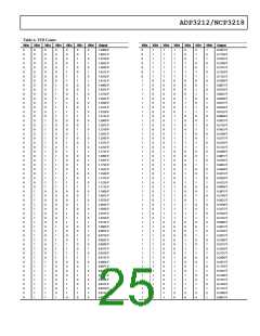
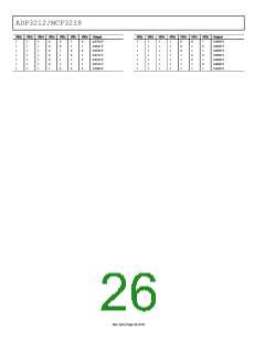
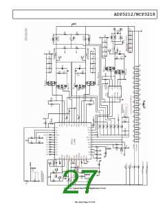
ADP3212/NCP3218
APPLICATION INFORMATION
The design parameters for a typical IMVP-6.5-compliant CPU
core VR application are as follows:
SETTING THE SWITCHING FREQUENCY FOR
RPM OPERATION OF PHASE 1
During the RPM operation of Phase 1, the ADP3212/NCP3218
runs in pseudoconstant frequency if the load current is high
enough for continuous current mode. While in DCM, the
switching frequency is reduced with the load current in a linear
manner.
•
•
•
•
•
•
•
Maximum input voltage (VINMAX) = 19 V
Minimum input voltage (VINMIN) = 8 V
Output voltage by VID setting (VVID) = 1.05 V
Maximum output current (IO) = 52 A
Droop resistance (RO) = 1.9 mΩ
Nominal output voltage at 40 A load (VOFL) = 0.9512 V
Static output voltage drop from no load to full load
(ΔV) = VONL − VOFL = 1.05 V − 0.9512 V = 98 mV
Maximum output current step (ΔIO) = 52 A
Number of phases (n) = 2
To save power with light loads, lower switching frequency is
usually preferred during RPM operation. However, the VCORE
ripple specification of IMVP-6.5 sets a limitation for the lowest
switching frequency. Therefore, depending on the inductor and
output capacitors, the switching frequency in RPM can be equal
to, greater than, or less than its counterpart in PWM.
•
•
•
•
•
Switching frequency per phase (fSW) = 300 kHz
Duty cycle at maximum input voltage (DMAX) = 0.13 V
Duty cycle at minimum input voltage (DMIN) = 0.055 V
SETTING THE CLOCK FREQUENCY FOR PWM
A resistor from RPM to GND sets the pseudo constant
frequency as following:
In PWM operation, the ADP3212/NCP3218 uses a fixed-
frequency control architecture. The frequency is set by an
external timing resistor (RT). The clock frequency and the
number of phases determine the switching frequency per phase,
which relates directly to the switching losses and the sizes of the
inductors and input and output capacitors. For a dual-phase
design, a clock frequency
of 600 kHz sets the switching frequency to 300 kHz per phase.
This selection represents the trade-off between the switching
losses and the minimum sizes of the output filter components.
To achieve a 600 kHz oscillator frequency at a VID voltage of
1.2 V, RT must be 181 kΩ. Alternatively, the value for RT can
be calculated by using the following equation:
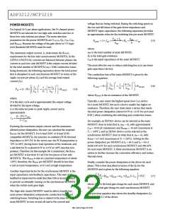
2× RT
VVID +1.0V
AR ×(1− D)×VVID
RR ×CR × fSW
(3
− 0.5kΩ
RRPM
=
×
)where:
AR is the internal ramp amplifier gain.
CR is the internal ramp capacitor value.
RR is an external resistor on the RAMPADJ pin to set the
internal ramp magnitude.
SOFT START AND CURRENT LIMIT
LATCH-OFF DELAY TIMES
INDUCTOR SELECTION
VVID +1V
2× n× fSW ×9pF
RT =
−16kΩ
(1)
The choice of inductance determines the ripple current of the
inductor. Less inductance results in more ripple current, which
increases the output ripple voltage and the conduction losses in the
MOSFETs. However, this allows the use of smaller-size inductors,
and for a specified peak-to-peak transient deviation, it allows
less total output capacitance. Conversely, a higher inductance
results in lower ripple current and reduced conduction losses,
but it requires larger-size inductors and more output capacitance
for the same peak-to-peak transient deviation. For a multiphase
converter, the practical value for peak-to-peak inductor ripple
current is less than 50% of the maximum dc current of that
inductor. Equation 4 shows the relationship between the
inductance, oscillator frequency, and peak-to-peak ripple
current. Equation 5 can be used to determine the minimum
inductance based on a given output ripple voltage.
where:
9 pF and 16 kΩ are internal IC component values.
VID is the VID voltage in volts.
n is the number of phases.
SW is the switching frequency in hertz for each phase.
V
f
For good initial accuracy and frequency stability, it is
recommended to use a 1% resistor.
When VARFREQ pin is connected to ground, the switching
frequency does not change with VID. The value for RT can be
calculated by using the following equation.
1V
RT =
−16kΩ
(2)
n×2× fSW ×9pF
VVID ×(1− DMIN
)
IR
=
(4)
fSW ×L
Rev. SpA | Page 28 of 43

 ONSEMI [ ONSEMI ]